CSCMV Overview
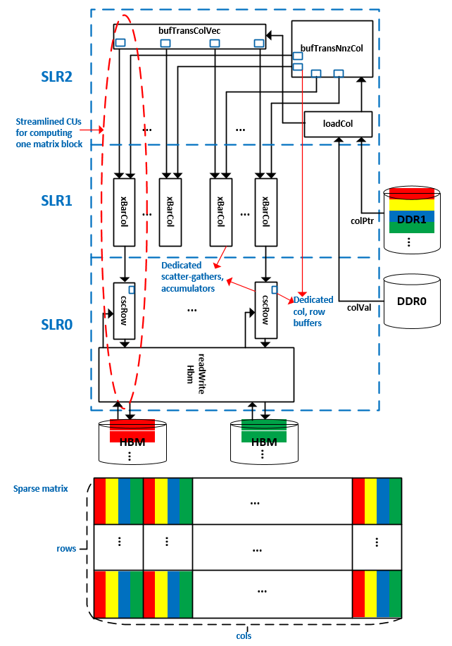
As shown in the figure below, the CSCMV accelerator implemented on the Alveo U280 card consists of a group of CUs (compute units, the instances of Vitis Kernels) connected via AXI STREAMs. In this design, 16 (out ot 32) HBM channels are used to store a sparse matrix NNZ values and row indices. Each HBM channel drives a dedicated computation path involving xBarCol and cscRow to perform the SpMV operation for the portion of the sparse matrix data stored in this HBM channel. In total, 16 SpMV operations are performed simultaneously for different parts of the sparse matrix data. Thanks to the CSC format storage of the sparse matrix, the input dense vector has a high degree of reusability. This reuability addressed in the bufTransColVec and bufTransNnzCol CUs and the low device memory access overhead addressed in the loadCol CU provide sufficient data throughput to allow the 16 parallel computattion paths to run at 300MHz to achieve highest performance. The highlights of this architecture are:
- Using AXI streams to connect a great number of CUs (37 CUs in this design) to allow massive parallelism being realized in the hardware
- Leveraging different device memories to reduce the memory access overhead and meet the computattion paths’ data throughput requirements
- Minimanizing the SLR (Super Logic Region) crossing logic to achieve higher clock rate
Although the above hardware architecture offers high computation power, it alone doesn’t provide a guarantee for the high system level performance. To achieve that, the sparse matrix data has to be partitioned evenly across the HBM channels. The following paragraghs present the details of the matrix partitioning strategy implemented in the software, the device memory layouts that facilitate the parition metadata decoding, the functionality of the CUs and the steps for building and simulating the design with Vitis 2020.2.
1. Matrix partitioning and device memory layout
As illustrated in the figure below, the matrix partitioning steps implemnted in the software are:
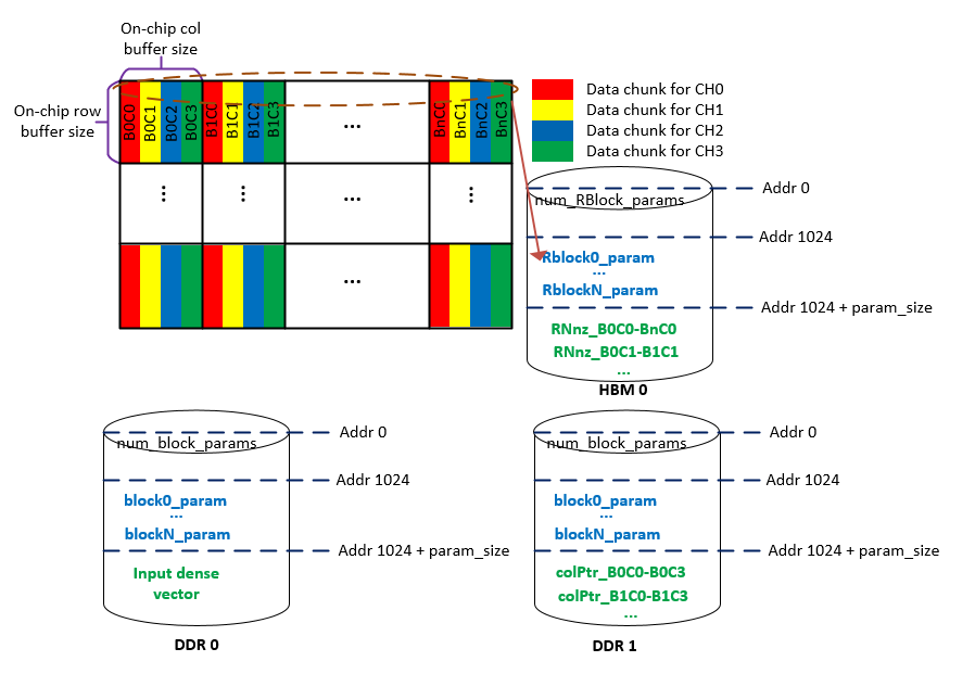
- Partition the entire matrix into blocks according to the on-chip row and column buffer sizes, shown as “on-chip row buffer size” and “on-chip col buffer size” in the figure. The “on-chip col buffer size” and the “on-chip row buffer size” can be defined at hardware compile time by macro
SPARSE_maxColMemBlocksandSPARSE_maxRowBlocks. For the Alveo U280 card, the following fomula shows how to compute the number of rows and columns in each on-chip matrix block.
number of columns in each block = SPARSE_maxColMemBlocks * 16
number of rows in each block = SPARSE_maxRowBlocks * 4
- Partition each block evenly into chunks along the column. The number of chuncks are decided at hardeware compile time by macro
SPARSE_hbmChannels. In this design 16 HBM channels are used. - According to their HBM channel ID, these data chunks are aseembled into different host memory regions, which will be migrated to different HBM channels on the device during runtime. For example, as shown in the figure above, the
reddata chunks in each block will be assembled into one memory block and migrated to HBM channel 0 on the device.
The matrix block partition information is stored in the DDR and HBM channels. The loadCol and readWriteHbm CUs will decode this information and retrieve the data correspondingly. As shown in the figure above, there are following three sections in each device memory.
Parameter summary section. This section is used to store number of parameter descriptions. The size (number of bytes) of this section is defined by macro
SPARSE_paramOffset, which is 1024 in the figure above.Parameter section. This section is used to store the parameter descriptions of data blocks. Each parameter description normally includes the address offset, the number of parallelly processed matrix/vector entries, the min/max indices in the blocks and etc.
Data section. This section is used to store matrix and vector data. The data inforamtion of DDR and HBM device memories are given below.
- DDR0: dense input vector data. Each DDR access produces 16 FP32 data entries.
- DDR1: column pointers of the NNZs in a sparse matrix. Each DDR access produces 16 column pointer values for 16 NNZs.
- HBM channels: row indices and values of the NNZs in a sparse matrix. Each access of one single HBM channels produces 4 values and 4 row indices data for 4 NNZs.
2. The functionality of the CUs
- The
loadColCU reads the input dense column vector and the NNZ column pointer entries from two physically separated DDR device memories DDR0 and DDR1 as shown in the figure above, and send them to thebufTransColVecandbufTransNnzColCUs to buffer and select entries for each computation path connected to each HBM channel. - The
bufTransColVecCU reads the input dense vector entries that belong to each block, split them into chuncks for each HBM channel, buffer all those chunks (16 in total in this design) and transmit the data to its correspondingxBarColCU. - The
bufTransNnzColCU reads the column pointer entries that belong to each block, split them into chuncks for each HBM channels, buffer all those chunks (16 in total in this design) and transmit the data to its correspondingxBarColCU. - The
xBarColCUs, one for each HBM channel, select the input dense vector entries according to the NNZs’ column pointer entries and send the result tocscRowCUs for computations. - Each
cscRowCU reads the value and row indices of NNZs from one HBM channel and multiplies the values with their corresponding column entries received from the connectedxBarColCU, and accumulates the results along the row indices. - Each
readWriteHbmCU connects to 8 HBM channels, and reads the NNZs’ value and row indices from those connected HBM channels and send the results to the correspondingcscRowCUs. It also collects the results from 8cscRowCUs and writes them back to the corresponding HBM channels. In total, 2readWriteHbmCUs are used to connect to 16 HBM channels.
3. Build and test the design
To build and test the design on Linux platform, please make sure your XILINX_VITIS and XILINX_XRT environment variables are set up correctly and point to the corresponding Vitis 2020.2 locations. Once your environment is set up properly, please navigate to the L2/tests/csmv directory and follow the steps below to run emulation and launch accelerator on Alveo U280.
- To run software emulation, please enter following commands. Please replace the $XILINX_VITIS with your Vitis 2020.2 installation location. The software emulation treats each CU as a dataflow module, and uses a wrapper called
cscmvSeqKernelas the top module to run the software emulation process. This is purely used for C++ level functionality test.
make cleanall
make run PLATFORM_REPO_PATHS=$XILINX_VITIS/platforms  DEVICE=$XILINX_VITIS/platform/xilinx_u280_xdma_201920_1/xilinx_u280_xdma_201920_1.xpfm  TARGET=sw_emu
- To run hardware emulation, please enter following commands. Please replace the $XILINX_VITIS with your Vitis 2020.2 installation location.
make cleanall
make run PLATFORM_REPO_PATHS=$XILINX_VITIS/platforms  DEVICE=$XILINX_VITIS/platform/xilinx_u280_xdma_201920_1/xilinx_u280_xdma_201920_1.xpfm  TARGET=hw_emu
- To build and launch the hardware accelerator on the Alveo U280, please enter following commands. Please replace the $XILINX_VITIS with your Vitis 2020.2 installation location.
make cleanall
make run PLATFORM_REPO_PATHS=$XILINX_VITIS/platforms  DEVICE=$XILINX_VITIS/platform/xilinx_u280_xdma_201920_1/xilinx_u280_xdma_201920_1.xpfm  TARGET=hw