Hardware Architecture of the Platform
Introduction
This section describes the design implemented on Processing System (PS) and Programmable Logic (PL) on the VMK180 board and the LIIMX274MIPI-FMC image sensor daughter card.
The following figure shows the top level hardware architecture of the reference design.
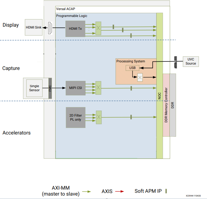
At a high level, the design comprises of three pipelines
Capture/Input pipeline: This comprises of pipelines through which video data are captured.
USB capture pipeline (PS)
MIPI CSI-2 capture pipeline (PL)
Display/Output pipeline: This comprises of pipelines through which video data are outputted.
DisplayPort pipeline (PL)
Video Accelerator/processing pipeline: This comprises of mem to mem pipelines through video data is processed/decrypted.
The 2D Filter accelerator (PL) integrated into the platform using Vitis.
VP9 Decoder and demux (PS)
Note: The PS interconnects in the figure are conceptual.
Capture
A capture pipeline receives video frames from an external source and writes it into memory. The single sensor MIPI CSI-2 receiver capture pipeline is shown in the following figure.
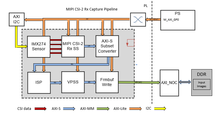
This pipeline consists of six components, four of which are controlled by the APU via an AXI4-Lite-based register interface, one is controlled by the APU via an I2C register interface, and one is configured statically.
The Sony IMX274 sensor is a 1/2.5 inch CMOS digital image sensor with an active imaging pixel array of 3864H x 2196V. The image sensor is controlled by an I2C interface using an AXI I2C controller in the PL. It is mounted on an FMC daughter card and has a MIPI output interface that is connected to the MIPI CSI-2 RX subsystem inside the PL. For more information, see the LIIMX274 MIPI FMC data sheet.
The MIPI CSI-2 receiver subsystem (CSI RX) includes a MIPI D-PHY core that connects four data lanes and one clock lane to the sensor on the FMC card. It implements a CSI-2 receive interface according to the MIPI CSI-2 standard v2.0 with underlying MIPI D-PHY standard v1.2. The subsystem captures images from the IMX274 sensor in RAW10 format and outputs AXI4-Stream video data. For more information, see the MIPI CSI-2 Receiver Subsystem Product Guide (PG232).
The AXI subset converter is a statically-configured IP core that converts the raw 10-bit (RAW10) AXI4-Stream input data to raw 8-bit (RAW8) AXI4-Stream output data by truncating the two least significant bits (LSB) of each data word.
The Image Single Processing IP available in the Vitis vision librarires (https://github.com/Xilinx/Vitis_Libraries/tree/master/vision/L1) implements the following functions. * The Badpixelcorrection module removes the defective pixels in the image as an image sensor may have a certain number of defective/bad pixels that may be the result of manufacturing faults or variations in pixel voltage levels based on temperature or exposure.
The Gain control module improves the overall brightness of the input image by applying a multiplicative gain (weight) for red and blue channel to the input bayerized image.
The Demosaicing module converts a single plane Bayer pattern output, from the digital camera sensors to a color image.
The histogram module computes the histogram of given input image. The normalization module changes the range of pixel intensity values. Both modules are used to improve the contrast in the image. See https://xilinx.github.io/Vitis_Libraries/vision/api-reference.html#vitis-vision-libraryfunctions for more details
The ISP IP receives the RAW AXI4-Stream input data and interpolates the missing color components for every pixel to generate a 24-bit, 8 bits per pixel (8 bpc) RGB output image transported via AXI4-Stream. At 4 ppc, the AXIS width is 96-bit. A GPIO from the PS is used to reset the IP between resolution changes.
The video processing subsystem (VPSS) is a collection of video processing IP sub-cores. This instance is uses the color space converter (CSC) configuration to perform color correction tasks including contrast, brightness, and red/green/blue gain control. The CSC takes AXI4-Stream input data and produces AXI4-Stream output data, both in 24-bit RGB format. A GPIO is used to reset the subsystem between resolution changes. For more information, see the Video Processing Subsystem Product Guide (PG231).
The video frame buffer takes YUV 4:2:0 sub-sampled AXI4-Stream input data and converts it to the memory mapped AXI4 format, which is written to memory as 12-bit packed YUYV. The memory mapped AXI interface is connected to the system DDR via the NoC. For each video frame transfer, an interrupt is generated. A GPIO is used to reset the IP between resolution changes.
All of the IPs in this pipeline are configured to transport 4 ppc, enabling up to 2160p60 performance.
Display
The HDMI TX display pipeline (in the PL) is controlled by the video frame buffer read, which fetches the video layer from memory and sends the data to the HDMI TX subsystem. The HDMI TX subsystem processes data and sends it out to an external display device. The HDMI transmitter display pipeline is shown in the following figure.
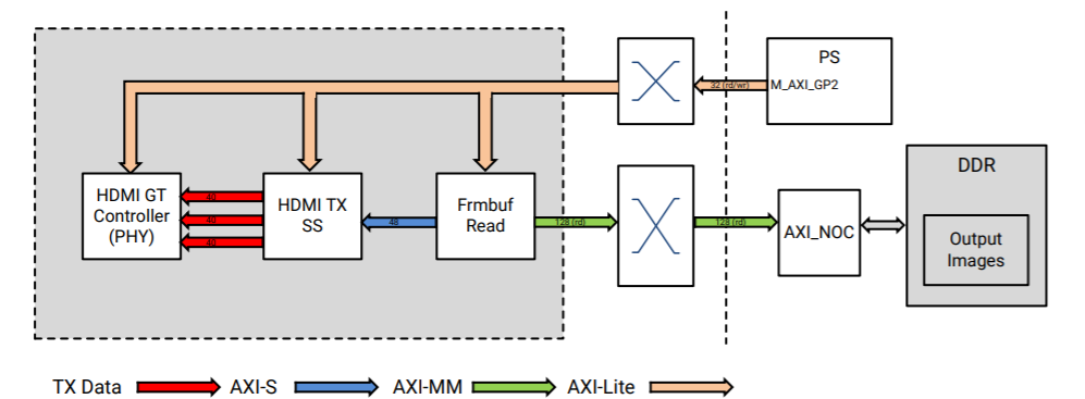
As shown in the figure, the pipeline comprises three main components, each of them controlled by the APU via an AXI4-Lite base register interface. These components are described in the following paragraphs.
The video frame buffer read IP provides high-bandwidth direct memory access between memory and AXI4-Stream video type target peripherals, which support the AXI4-Stream video protocol. IP takes memory mapped AXI4 input data from DDR and converts it to AXI4-Stream format. The output is connected to HDMI transmitter subsystem. For each video frame transfer, an interrupt is generated. A GPIO is used to reset the core between resolution changes. For more information, see the Video Frame Buffer Read and Video Frame Buffer Write LogiCORE IP Product Guide (PG278).
The HDMI transmitter subsystem (HDMI TX) interfaces with PHY layers and provides HDMI encoding functionality. The subsystem is a hierarchical IP that bundles a collection of HDMI TXrelated IP sub-cores and outputs them as a single IP. The subsystem generates an HDMI stream from the incoming AXI4-Stream video data and sends the generated TMDS data to the video PHY layer. For more information, see the HDMI 1.4/2.0 Transmitter Subsystem Product Guide (PG235).
The HDMI GT controller (PHY) enables plug-and-play connectivity with video transmit or receive subsystems. The interface between the media access control (MAC) and physical (PHY) layers are standardized to enable ease of use in accessing shared gigabit-transceiver (GT) resources. The data recovery unit (DRU) supports lower line rates for the HDMI protocol. An AXI4-Lite register interface is provided to enable dynamic accesses of transceiver controls/status. For more information, see the HDMI GT Controller LogiCORE IP Product Guide (PG334 <https://www.xilinx.com/support/documentation/ip_documentation/hdmi_gt_controller/v1_0/pg334-hdmi-gt-controller.pdf>_).
Clocks
PS Clocks
The following table lists the clock frequencies of key PS components.
Component |
Clock Frequency |
|---|---|
ACPU |
1,000 MHz |
NOC |
960 MHz |
NPI |
300 MHz |
LPDDR |
1,600 |
System Clocks
The following table identifies the main clocks of the PL design, their source, their clock frequency, and their function.
Clock |
Clock Source |
Clock Frequency |
Function |
|---|---|---|---|
pl0_ref_clk |
CIPS |
100 MHz |
Clock source for clocking wizard. |
clk_out1 |
Clocking wizard |
150 MHz |
Memory mapped AXI clock, accelerator clock. |
clk_out2 |
Clocking wizard |
105 MHz |
AXI-Lite clock to configure the different IPs in the design. |
clk_out3 |
Clocking wizard |
200 MHz |
MIPI D-PHY core clock, AXI4-Stream clock. |
sys_clk0 |
SI570 (External) |
200 MHz |
Differential clock source used internally by the memory controller to generate various clocks to access DDR memory. |
HDMI DRU clock |
SI570 (External) |
200 MHz |
Clock for data recovery unit for low line rates. |
The PL0 clock is provided by the PPLL inside the PMC domain and is used as the reference input clock for the clocking wizard instance inside the PL. This clock does not drive any loads directly. A clocking wizard instance is used to deskew the clock and to provide three phase-aligned output clocks, Clk_out1, Clk_100MHz, and Clk_200MHz.
The Clk_100MHz clock is generated by the clocking wizard instance. It is used to drive most of the AXI4-Lite control interfaces in the PL. AXI4-Lite interfaces are typically used in the control path to configure IP registers and, consequently, can operate at a lower frequency than datapath interfaces.
The Clk_out1 clock is generated by the clocking wizard instance. It is used to drive the memory mapped AXI interfaces of the capture pipelines in the PL. These interfaces are in the datapath and, consequently, are needed to support the maximum performance of 2160p60, which roughly corresponds to a 150 MHz clock at 4 ppc. The HLS-based IP core interfaces and Vitis generated modules are based on Clk_out1 rather than Clk_100MHz (HLS IPs typically share a common input clock between control and data interfaces).
Next Steps
License
Licensed under the Apache License, Version 2.0 (the “License”); you may not use this file except in compliance with the License.
You may obtain a copy of the License at [http://www.apache.org/licenses/LICENSE-2.0](http://www.apache.org/licenses/LICENSE-2.0)
Unless required by applicable law or agreed to in writing, software distributed under the License is distributed on an “AS IS” BASIS, WITHOUT WARRANTIES OR CONDITIONS OF ANY KIND, either express or implied. See the License for the specific language governing permissions and limitations under the License.