Embedded System Design Flow on Zynq
Labs outline
The purpose of This workshop is to walk you through a complete hardware and software processor system design. It provides participants the necessary skills to develop complex embedded systems and enable them to improve their designs by using the tools available in Vivado and Vitis IDE. It also helps developers understand and utilize advanced components of embedded systems design for architecting a complex system in the Zynq™ System on a Chip (SoC)
Source Files Setup
To use the source files for each of the labs in this workshop, you have to download or clone this repository from GitHub.
On the main GitHub webpage for a repository, you can select Clone or download and select Download Zip to download an archive of the repository. You can then extract this to a folder on your local machine.
If you prefer to use git you can clone this repository:
git clone https://github.com/Xilinx/xup_embedded_system_design_flow
In the instructions for the labs;
{sources} refers to the ./sources directory in this respoitory once you have copied or cloned it to a local directory.
{labs} refers to the location which you will use as your workspace for the labs in the workshop.
{Vitis_Workspace} refers your workspace directory to launch Vitis IDE.
NOTE
Board support for PYNQ-Z2 are not included in Vivado by default. The relevant files need to be extracted and saved to: {Vivado installation}\data\boards\board_files\
If you do not see the board_files folder, create it manually.
These files can be downloaded from
PYNQ-Z2:/board_files.
Hardware Setup
PYNQ-Z2: Connect a micro USB from the board to the PC. Make sure that a jumper is connected to JTAG (between JP1_1 and JP1_2) and another one of them should be connected across the USB pins (between J9_2 and J9_3).
Extra Resources:
The Zynq book can be used to find more information about Zynq technology that is seen in these labs. It is available for free download at http://www.zynqbook.com/.
Labs Overview:
Lab 1
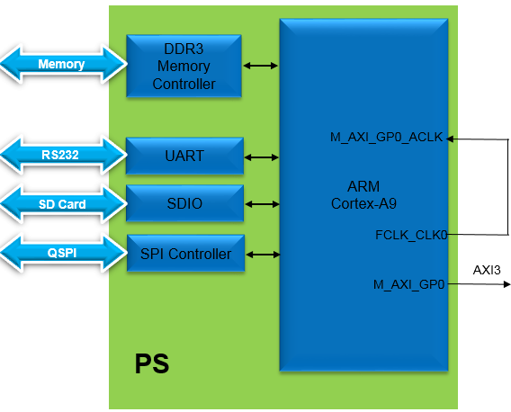
In this lab, you will use IP Integrator to create a processing system based design consisting of the following :
- ARM Cortex A9 core (PS)
- UART for serial communication
-
DDR3 controller for external DDR3_SDRAM memory
Processor Design of this Lab
Lab 2
This lab guides you through the process of extending the processing system you created in the previous lab by adding two GPIO (General Purpose Input/Output) IPs.
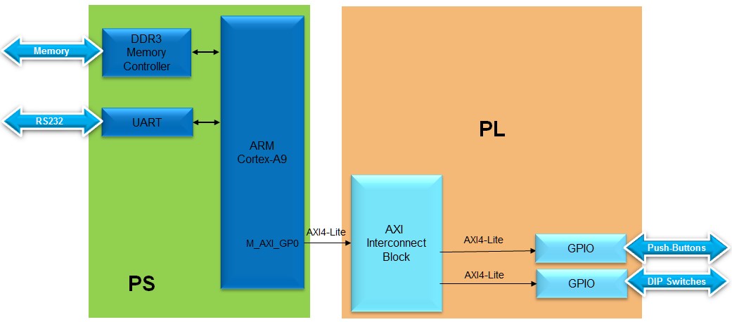
Extend the System from the Previous Lab
Lab 3
This lab guides you through the process of creating and adding a custom peripheral to a processor system by using the Vivado IP Packager. You will create an AXI4Lite interface peripheral.
You will extend the Lab 2 hardware design by creating and adding an AXI peripheral to the system, and connecting it to the LEDs on the Zynq board you are using. You will use the IP Packager to generate the custom IP. Next, you will connect the peripheral to the system and add pin location constraints to connect the LED display controller peripheral to the on-board LED display. Finally, you will add BRAM Controller and BRAM before generating the bitstream.
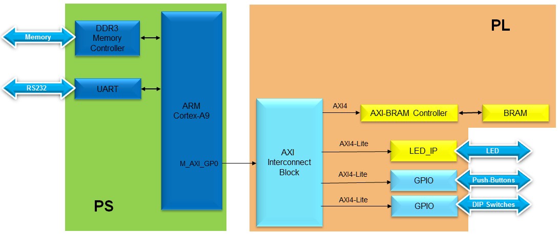
Design updated from the previous lab
Lab 4
This lab guides you through the process of writing a basic software application. The software you will develop will write to the LEDs on the Zynq board. An AXI BRAM controller and associated 8KB BRAM were added in the last lab. The application will be run from the BRAM by modifying the linker script for the project to place the text section of the application in the BRAM. You will verify that the design operates as expected, by testing in hardware.
The design was extended at the end of the previous lab to include a memory controller, and the bitstream should now be available. A basic software application will be developed to access the LEDs on the Zynq boards.
Lab 5
This lab guides you through the process of writing a software application that utilizes the private timer of the CPU. You will refer to the timer’s API in the Vitis IDE to create and debug the software application. The application you will develop will monitor the dip switch values and increment a count on the LEDs. The application will exit when the center push button is pressed.
You will use the hardware design created in lab 4 to use CPU’s private timer (see Figure). You will develop the code to use it.

Final design
Lab 6
Software and hardware interact with each other in an embedded system. The Vitis includes System Debugger as a software debugging tool. The hardware analyzer tool has different types of cores that allow hardware debugging by providing access to internal signals without requiring the signals to be connected to package pins. These hardware debug cores may reside in the programmable logic (PL) portion of the device and can be configured with several modes that can monitor signals within the design. In this lab you will be introduced to the various debugging cores.
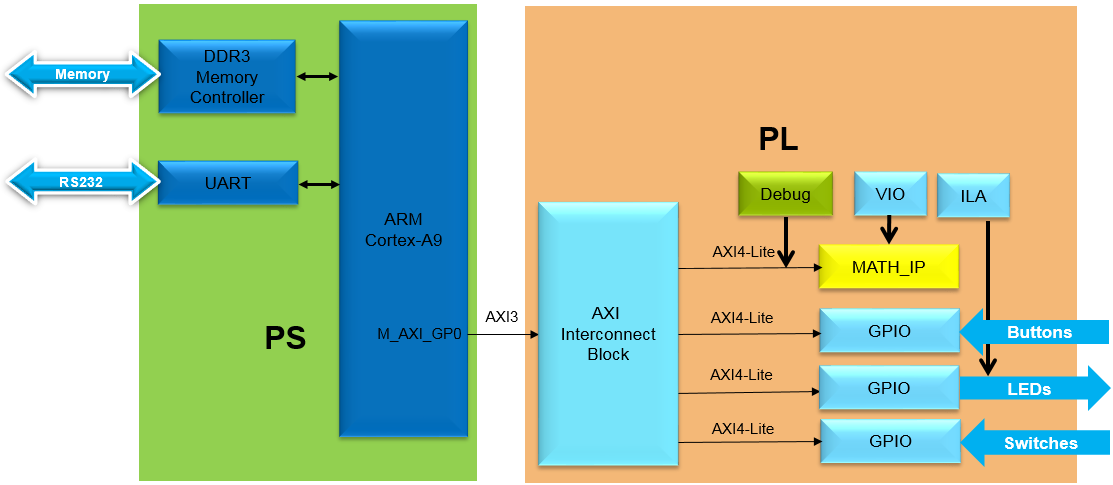
Lab 7
In Zynq, multiple interconnections are available between the PS and PL sections with different performance levels for data transfer between the two subsystems. The General Purpose (GP) Master and Slave AXI interconnect used in the previous labs are intended for peripherals that do not have high bandwidth requirements. E.g. switches, leds, keyboard, mouse. There are four High Performance PS slave to PL master AXI interfaces available for peripherals that need higher bandwidth. E.g. Video and image processing applications. This lab guides you through the process of enabling a High Performance AXI slave port in the PS, adding an AXI central DMA (CDMA) controller, and performing Direct Memory Access (DMA) operations between various memories.
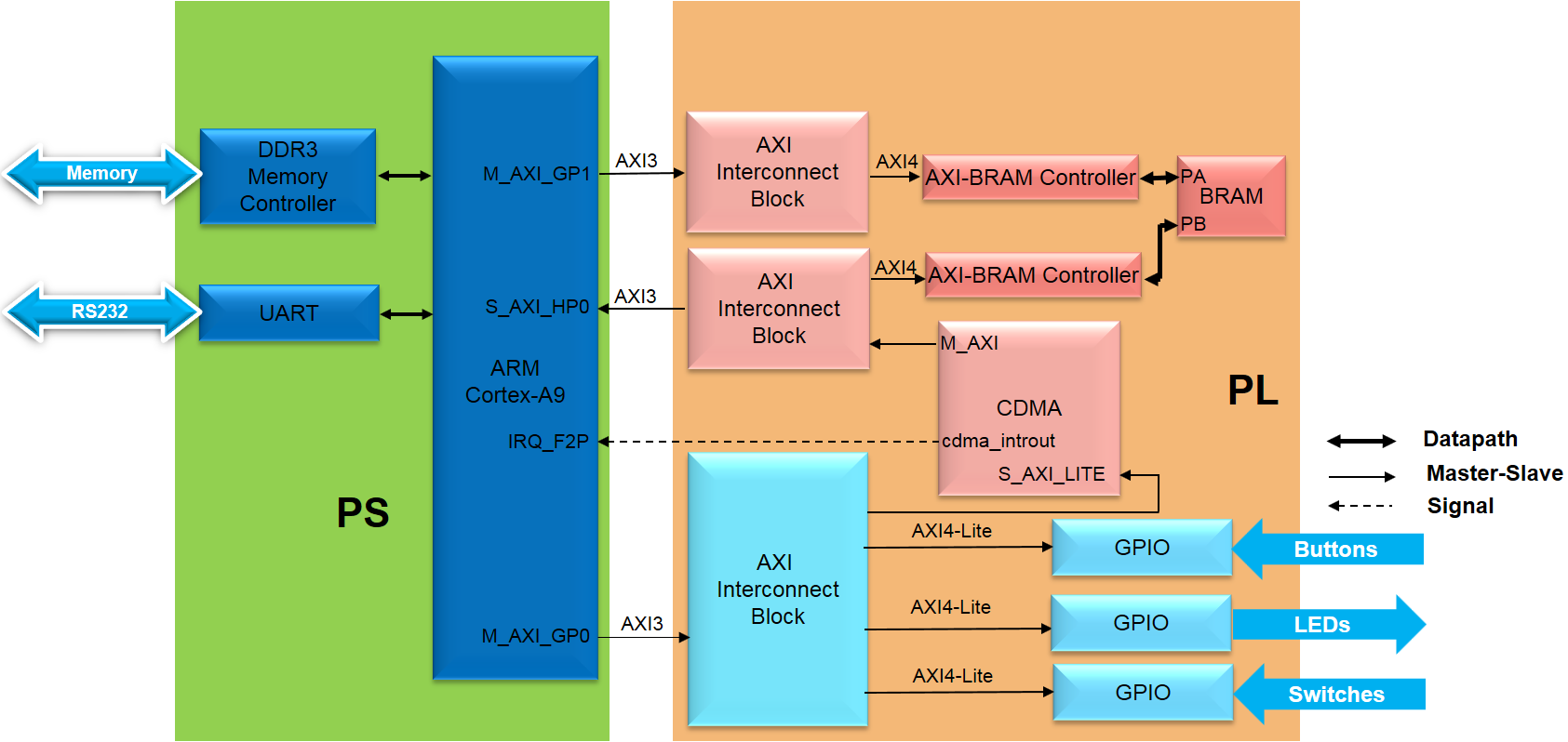
Lab 8
This lab guides you through creating a bootable system capable of booting from the SD card or the QSPI flash memory located on the board. It also demonstrates how different bitstreams can be loaded in the PL section after the board is booted up and the corresponding application can be executed.
