Adding IP cores in PL
Objectives
After completing this lab, you will be able to:
- Configure the GP Master port of the PS to connect to IP in the PL.
- Add additional IP to a hardware design.
- Setup some of the compiler settings.
Steps
Open the Project
- Open the previous project.
- Select File > Project > Save As… to open the Save Project As dialog box. Enter lab2 as the project name. Make sure that the Create Project Subdirectory option is checked, the project directory path is {labs} and click OK. This will create the lab2 directory and save the project and associated directory with lab2 name.
Add Two Instances of GPIO
- In the Sources panel, expand system_wrapper, and double-click on the system.bd (system_i) file to invoke IP Integrator.
- Double click on the Zynq block in the diagram to open the Zynq configuration window.
- Select PS-PL Configuration page menu on the left.
- Expand AXI Non Secure Enablement > GP Master AXI Interfaces, if necessary, and click on Enable M_AXI_GP0 interface check box under the field to enable the AXI GP0 port.
- Expand General > Enable Clock Resets and select the FCLK_RESET0_N option.
- Select the Clock Configuration tab on the left. Expand the PL Fabric Clocks and select the FCLK_CLK0 option (with requested clock frequency of 100.000000 MHz) and click OK.
- Notice the additional M_AXI_GPO interface, and M_AXI_GPO_ACLK, FCLK_CLK0, and FCLK_RESET0_N ports are now included on the Zynq block. You can click the regenerate button to redraw the diagram to get something like this:
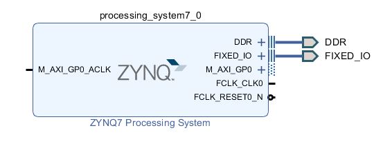
Zynq system with AXI and clock interfaces
-
Next add an IP by right clicking on the Diagram window> Add IP and search for AXI GPIO in the catalog.
-
Double-click the AXI GPIO to add the core to the design. The core will be added to the design and the block diagram will be updated.
-
Click on the AXI GPIO block to select it, and in the properties tab, change the name to switches.
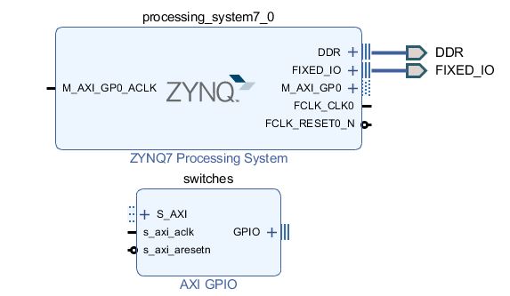
Change AXI GPIO default name
- Double click on the AXI GPIO block to open the customization window.
- Click the Board tag, From the Board Interface drop down, select sws 2bits for GPIO IP Interface. Leave GPIO as default setting.
-
Next, click the IP configuration tab, and notice the width has already been set to match the switches on the PYNQ-Z2 (2)
Notice that the peripheral can be configured for two channels, but, since we want to use only one channel without interrupt, leave the Enable Dual Channel and Enable Interrupt unchecked.
Channels here just refer to wired connections between peripherals and other components. Dual Channel would enable you to signals of 128 bits in lenght where has using one channel only allow for signals 64 bits in lenght. This option is to increase the bandwidth of the connection this periperhal could send.
- Click OK to save and close the customization window.
- Notice that Designer assistance is available. Click on Run Connection Automation, and select /switches/S_AXI
- Click OK when prompted to automatically connect the master and slave interfaces. Notice that two additional blocks, Processor System Reset, and AXI Interconnect have automatically been added to the design. (The blocks can be dragged to be rearranged, or the design can be redrawn).
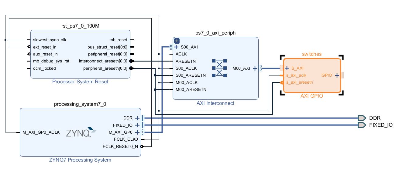
Design with switches automatically connected
- Add another instance of the GPIO peripheral (Add IP). Name it as buttons.
-
Double click on the IP block, in the GPIO interface select btns 4bits for the PYNQ-Z2, click OK.
At this point connection automation could be run, or the block could be connected manually. This time the block will be connected manually.
-
Double click on the AXI Interconnect (name : ps7_0_axi_periph) and change the Number of Master Interfaces to 2 and click OK
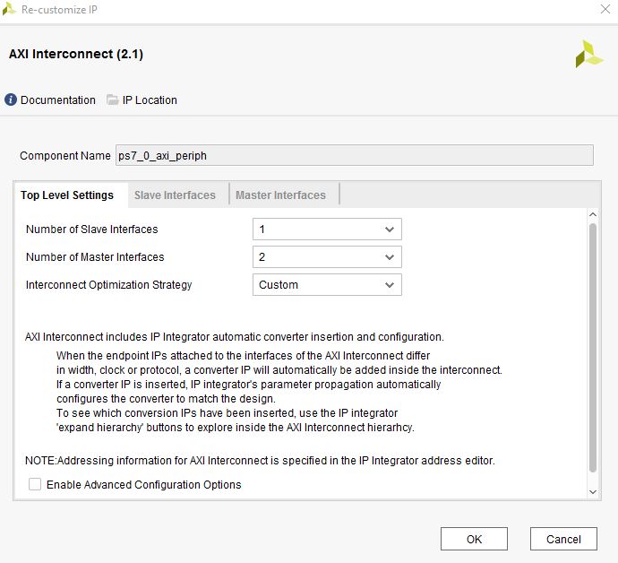
Add master port to AXI Interconnect
-
Click on the s_axi port of the buttons AXI GPIO block (name: buttons), and drag the pointer towards the AXI Interconnect block.
The message “Found 1 interface” should appear, and a green tick should appear beside the M01_AXI port on the AXI Interconnect indicating this is a valid port to connect to. Drag the pointer to this port and release the mouse button to make the connection.
-
In a similar way, connect the following ports:
buttons s_axi_aclk -> Zynq7 Processing System FCLK_CLK0
This ensures that the Zynq proccessing system and the peripherals communicate synchronously. (Can you remember what frequency we set the proccessor clock to?).
buttons s_axi_aresetn -> Processor System Reset peripheral_aresetn.
The Zynq proccesing system controls the reset to the peripherals.
AXI Interconnect M01_ACLK -> Zynq7 Processing System FCLK_CLK0.
AXI Interconnect M01_ARESETN -> Processor System Reset peripheral_aresetn.
The block diagram should look similar to this:
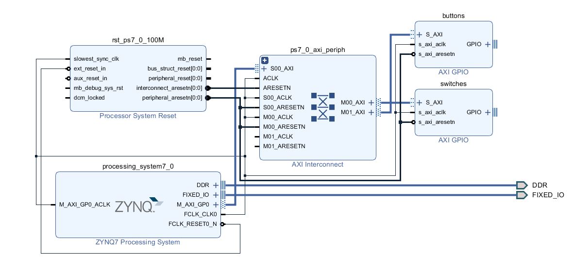
System Assembly View after Adding the Peripherals
- Click on the Address Editor tab, and expand processing_system7_0/Data > Unassigned Slaves if necessary.
- Notice that switches has been automatically assigned an address, but buttons has not (since it was manually connected). Right click on /buttons/S_AXI and select Assign.
Note that both peripherals are assigned in the address range of 0x40000000 to 0x7FFFFFFF (GP0 range).
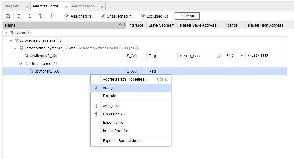
Peripherals Memory Assign
Make GPIO Peripheral Connections External
- In the Diagram view, notice that Designer Assistance is available. We will manually create the ports and connect.
- Right-Click on the GPIO port of the switches instance and select Make External to create the external port. This will create the external port named GPIO_0 and connect it to the peripheral. Because Vivado is “board aware”, the pin constraints will be automatically applied to the port.
- Select the GPIO_0 port and change the name to switches in its properties form. The width of the interface will be automatically determined by the upstream block.
- For the buttons GPIO, click on the Run Connection Automation link.
- In the opened GUI, select btns_4bits (for PYNQ-Z2) under the options section.
- Click OK.
- Select the created external port and change its name to buttons.
-
Run Design Validation (Tools -> Validate Design) and verify there are no errors.
The design should now look similar to the diagram below
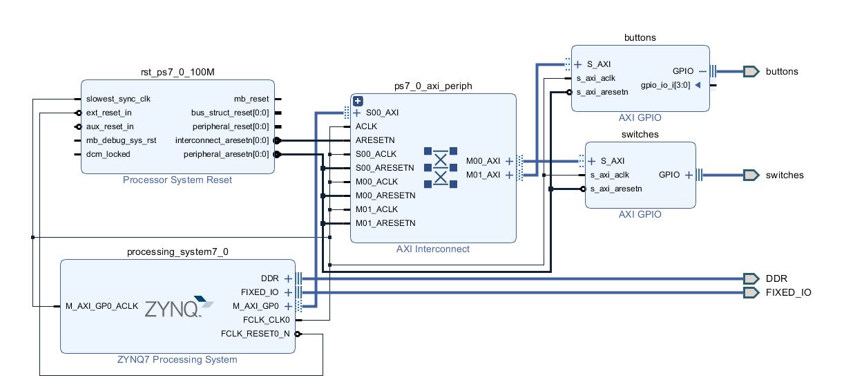
Completed design
- In the Flow Navigator, click Run Synthesis. (Click Save if prompted) and when synthesis completes, select Open Synthesized Design and click OK
- In the shortcut Bar, select I/O Planning from the Layout dropdown menu
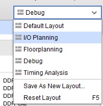
Switch to the IO planning view
- In the I/O ports tab, expand the two GPIO icons, and expand buttons_tri_i, and switches_tri_i, and notice that the ports have been automatically assigned pin locations, along with the other Fixed IO ports in the design, and an I/O Std of LVCMOS33 (PYNQ-Z2) has been applied. If they were not automatically applied, pin constraints can be included in a constraints file, or entered manually or modified through the I/O Ports tab.
If buttons_tri_i, and switches_tri_i do not appear in the I/O ports tab open Elaborated Design and check to see if they are grounded. If they are grounded please a mistake was likely made in configuring this system. Please repeat the previous steps carefully!.
Generate Bitstream and Export Hardware
- Click on Generate Bitstream, and click Yes if prompted to Launch Implementation (Click Yes if prompted to save the design).
- Click Cancel.
- Export the hardware by clicking File > Export > Export Hardware and click OK. This time, there is hardware in Programmable Logic (PL) and a bitstream has been generated and should be included in the export.
- Click Yes to overwrite the hardware module.
Generate TestApp Application in Vitis IDE
- Start Vitis IDE by clicking Tools > Launch Vitis IDE and click OK.
- Right click on the previous application project (lab1_system) from the Explorer view and select Close System Project.
- From the File menu select File > New > Application Project. Click Next to skip the welcome page if necessary.
- In the Platform Selection window, select Create a new platform from hardware (XSA) and browse to select the {labs}\lab2\system_wrapper.xsa file exported before.
- Enter lab2platform** as the _Platform name, click **Next.
- Name the project lab2, click Next.
- Select standalone_ps7_cortexa9_0, click Next.
- Select Empty Application(C) and click Finish.
- Expand lab2_system > lab2 in the Explorer view, and right-click on the src folder, and select Import Sources….
- Browse to select the {sources}\lab2 folder, click Open Folder.
- Select lab2.c and click Finish.
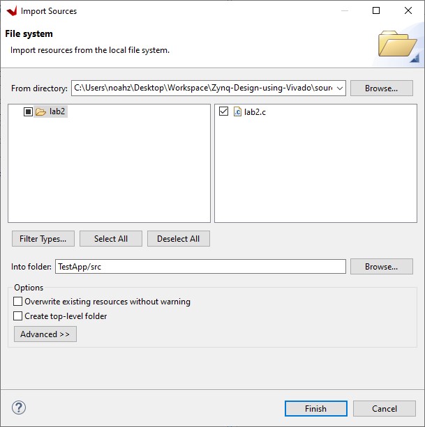
Import resources from the local file system
- Build the project either by clicking the hammer button or by right-clicking on the application project and selecting Build Project.
Test in Hardware
- Make sure that micro-USB cable(s) is(are) connected between the board and the PC. Change the boot mode to JTAG. Turn ON the power of the board. >To changed the PYNQ-Z2’s boot mode to JTAG, locate the JTAG pins on the board beside the HDMI input port. There should be a dark gray removable pin connector on two of the pins. Make sure that this connector is connect to the JTAG pins which are the right two pins on the horizontal rows.
- Open a serial communication utility for the COM port assigned on your system. The Vitis software platform provides a serial terminal utility will be used throughout the tutorial. You can also use your preferred serial terminal application.
- To open this utility, select Window > Show view.
- In the Show View dialog box, type terminal in the search box.
- Select Vitis Serial Terminal and click Open.
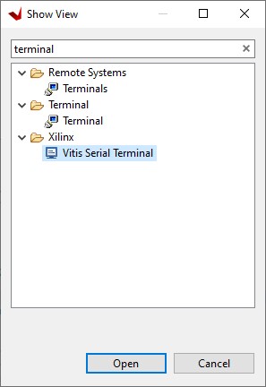
Open the Vitis Serial Terminal
- Click the Add button in the Vitis Serial Terminal to connect to a serial terminal. Select the port from the dropdown menu. Keep the Advanced Settings as-is. Click OK.
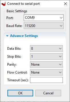
Connect to serial port
-
Right-click lab2_system > lab2 and select Launch Hardware (Single Application Debug).
- Play with the buttons and switches, you should see the following output on the Terminal tab.
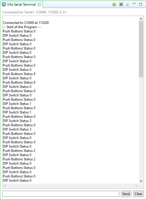
Connect to serial port
- Close Vivado and Vitis IDE by selecting File > Exit in each program.
Conclusion
GPIO peripherals were added from the IP catalog and connected to the Processing System through the 32b Master GP0 interface. The peripherals were configured and external FPGA connections were established. A TestApp application project was created and the functionality was verified after downloading the bitstream and executing the program.