Direct Memory Access using CDMA
Objectives
After completing this lab, you will be able to:
- Enable a High Performance (HP) port of the processing system.
- Add and connect the CDMA controller in the programmable logic.
- Perform DMA operation between various memories.
Steps
Open the Project
- Start Vivado if necessary and open the lab2 project (lab2.xpr) you created in the previous lab.
- Select File > Project > Save As … to open the Save Project As dialog box. Enter lab7 as the project name. Make sure that the Create Project Subdirectory option is checked, the project directory path is {labs} and click OK.
Add GPIO Instance for LEDs
- Click Open Block Design in the Flow Navigator pane to open the block diagram.
- Add an AXI GPIO IP by right clicking on the Diagram window > Add IP and search for AXI GPIO in the catalog, rename it to leds.
- Double click on the leds block, and select leds 4bits for the GPIO interface and click OK.
- Click Run Connection Automation, and select leds (which will include GPIO and S_AXI). Click on GPIO and S_AXI to check the default connections for these interfaces.
- Click OK to automatically connect the S_AXI interface to the Zynq GP0 port (through the AXI interconnect block), and the GPIO port to an external interface. Rename the port leds_4bits to leds.
Configure the Processor
- Double-click on the Zynq processing system instance to open its configuration form.
- Select PS-PL Configuration in the Page Navigator window in the left pane, expand HP Slave AXI Interface on the right, and click on the check-box of the S AXI HP0 Interface to enable it.
- Expand AXI Non Secure Enablement > GP Master AXI Interface and enable the M AXI GP1 Interface.
- Select Clock Configuration in the Page Navigator window in the left pane, expand PL Fabric Clocks on the right, enable the FCLK_CLK1. Enter the Requested Frequency for the FCLK_CLK1 as 140 MHz.
- Click OK to accept the settings and close the configuration form.
Add CDMA and BRAM
Instantiate the AXI central DMA controller.
- Click the Plus button or right click the Diagram window and select Add IP, search for Central in the catalog. Double-click the AXI Central Direct Memory Access to add an instance to the design.
- Double-click on the axi_cdma_0 instance and uncheck the Enable Scatter Gather option.
-
Change the Write/Read Data Width to 64 and click OK.
Note the burst size changes from 16 to 8. You can increase this up to 256 to improve the performance. Here we are using smallest number since the application allows small number of words transfer.
Run connection automation
Connection automation could be run on all unconnected ports simultaneously. For the purposes of this lab, each port will be connected separately so that the changes made by the automation process are easier to follow.
- Click on Run Connection Automation and select processing_system7_0/S_AXI_HP0
- Check that this port will be connected to the /axi_cdma_0/M_AXI port and click OK.
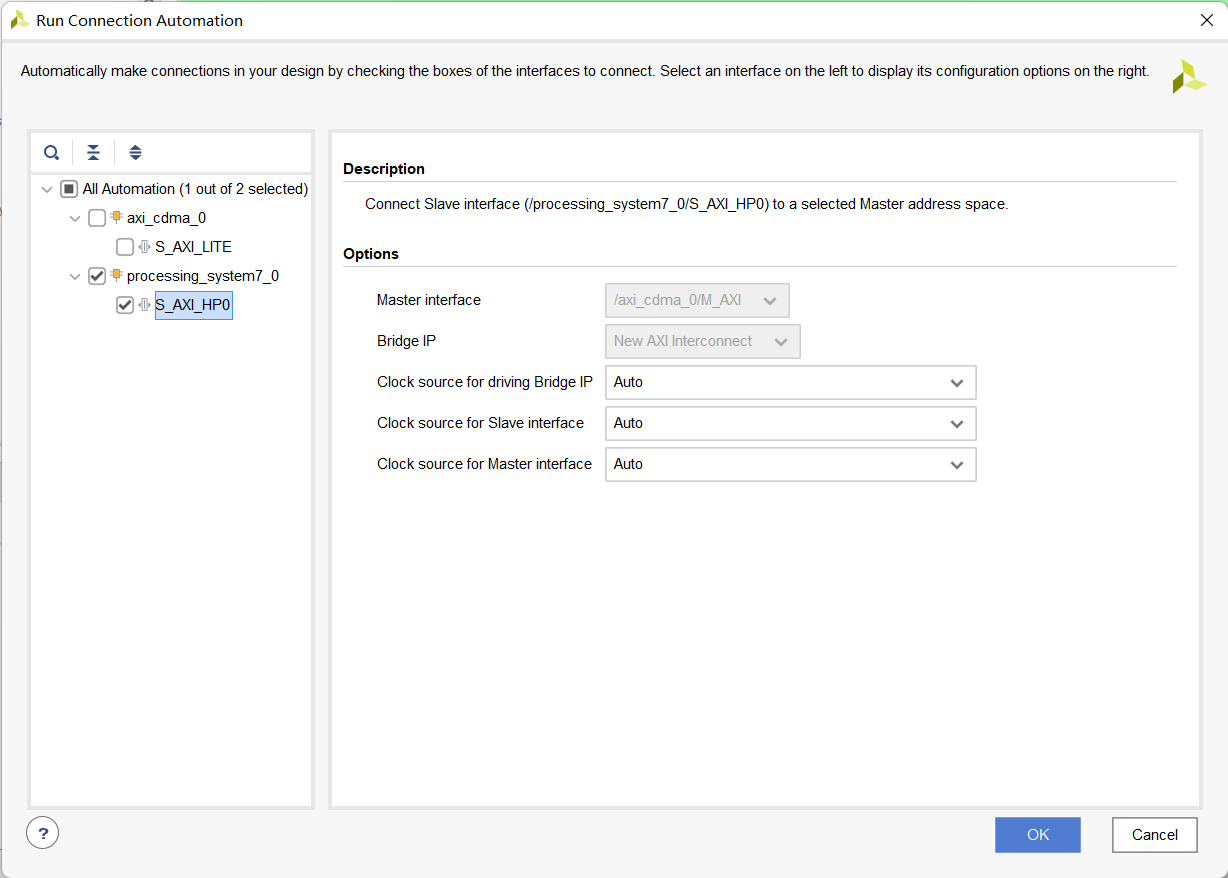
Connection automation
- Verify the CDMA connection through the AXI SmartConnect to the HP0 port

Connecting AXI Central DMA controller to S_AXI_HP0
Notice that an instance of AXI SmartConnect (axi_smc_1) is added, S_AXI_HP0 of the processing_system7_0 is connected to M00_AXI of the axi_smc_1, S00_AXI of the axi_smc_1 is connected to the m_axi of the axi_cdma_0 instance. Also, m_axi_aclk of the axi_cdma_0 is connected to the net originating from FCLK_CLK0 of the processing_system7_0.
-
Click on Run Connection Automation again, and select /axi_cdma_0 (which includes S_AXI_LITE ). Click OK.
Notice that the axi_cdma_0/M_AXI port is no longer available to select. This is because it was connected to the processing system in the previous step.
Instantiate two BRAM Controllers and BRAMs.
- Click the Add button or right click the Diagram window and select Add IP, search for BRAM in the catalog. Double-click the AXI BRAM Controller to add an instance to the design.
- Click on Run Connection Automation , and select axi_bram_ctrl_0
- Click on BRAM_PORTA and BRAM_PORTB check boxes.
- Click S_AXI , and change the Master Interface option to /processing_system7_0/M_AXI_GP1, change the Clock source for driving interconnect IP, Clock source for Master interface, and Clock source for Salve interface to /processing_system7_0/FCLK_CLK1 (140 MHz) as they all run in the same clock domain, and click OK.
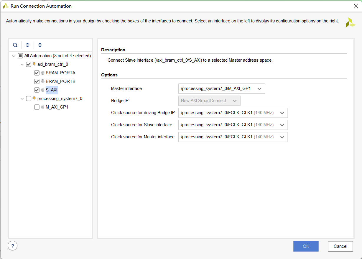
Connecting AXI BRAM Controller to M_AXI_GP1 to run at faster clock speed
Notice that an instance of AXI SmartConnect and Processor System Reset are added, and the M_AXI_GP1_ ACLK is connected to FCLK_CLK1.
- Add another AXI BRAM Controller by Clicking the Add button and search for BRAM.
- Click on Run Connection Automation , and select /axi_bram_ctrl_1/S_AXI only.
- For the Master connection, select axi_cdma_0/M_AXI from the dropdown box.
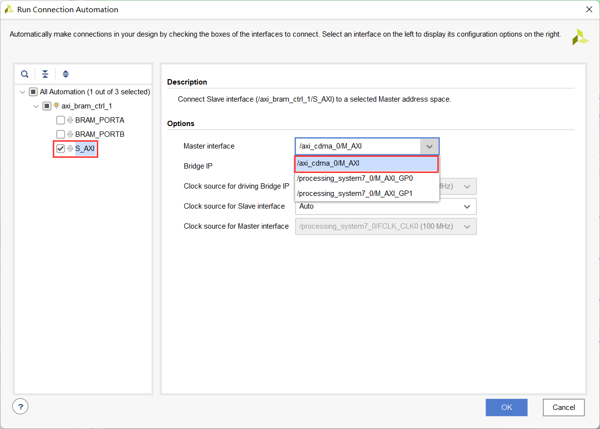
BRAM Connection Automation
- Click OK to make the connection.
- Double-click the axi_bram_ctrl_1 instance and change the Number of BRAM Interface to 1. Change the Data Width to 64 and click OK.
- Double-click the axi_bram_ctrl_0 instance and also change the Number of BRAM Interface to 1 and change the Data Width to 64. Click OK.
- Using the wire tool, connect the BRAM_PORTA of the axi_bram_ctrl_1 instance to the BRAM_PORTB of the Block Memory Generator axi_bram_ctrl_0_bram instance.

Connect the second BRAM controller
Connect the CDMA interrupt out port to the port of the processor.
- Double-click on the processing_system7_0 instance to open its configuration form.
- Select Interrupts in the Page Navigator window in the left pane, check the Fabric Interrupts box.
- Expand Fabric Interrupts > PL-PS Interrupts Ports, and click on the check-box of the IRQ_F2P.

Enabling the processor interrupt
- Click OK.
- Using wiring tool, connect the cdma_introut to the IRQ_F2P port. (Click on the cdma_introut port and drag to the IRQ_F2P port)
Set the BRAM controller size to 64KB.
- Select the Address Editor tab.
- Expand the axi_cdma_0> Data section, and change the memory size of axi_bram_ctrl_1 to 64K.

Address space
- The design should look similar to the figure below.
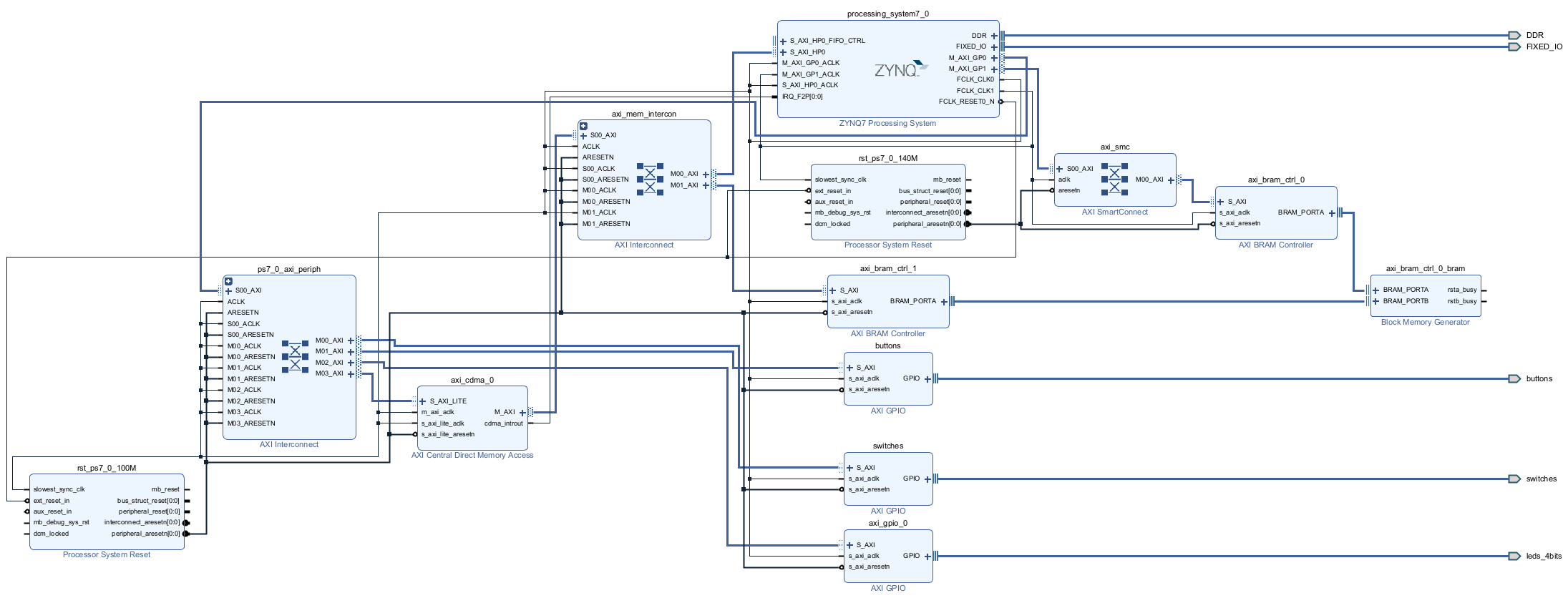
Completed design
- Select the Diagram tab, and click on the Validate Design (F6) button to make sure that there are no errors.
Generate the Bitstream
- Click on the Generate Bitstream to run the synthesis, implementation, and bit generation processes.
- Click Save to save the project, and Yes if prompted to run the processes. Click OK to launch the runs.
- When the bitstream generation process has completed successfully, click Cancel.
Generate an Application in Vitis IDE
Export the implemented design, and start SDK
- Export the hardware configuration by clicking File > Export > Export Hardware…
- Click the box to Include Bitstream and click OK (Click Yes if prompted to overwrite a previous module).
- Launch Vitis IDE by clicking Tools > Launch Vitis IDE and click OK.
- To clean the workspace, right-click on each opened system project and select Close System Project.
Create an empty application project, named lab7, and import the provided lab7.c file.
- From the File menu select File > New > Application Project. Click Next to skip the welcome page if necessary.
- In the Platform Selection window, select Create a new platform from hardware (XSA) and browse to select the {labs}\lab7\system_wrapper.xsa file exported before.
- Enter lab7platform** as the _Platform name, click **Next.
- Name the project lab7, click Next.
- In the domain selection window, select standalone_ps7_cortexa9_0, click Next.
- In the templates selection window, select Empty Application(C), click Finish.
- Expand lab7 in the Explorer view, and right-click on the src folder, and select Import Sources….
- Browse to select the {sources}\lab7 folder, click Open Folder.
- Select lab7.c and click Finish.
- Build the project either by clicking the Hammer button or right-clicking on lab7 from Explorer View and selecting Build Project.
Test in Hardware
Establish serial communication
- Connect and power up the board with JTAG mode.
- Click Window > Show View, search and open Vitis Serial Terminal.
- Click the Add button to connect to a port.
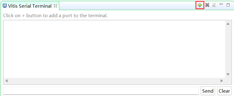
Add a Serial Port
- Select the Port from the dropdown menu. Keep the Advanced Settings as-is. Click OK.
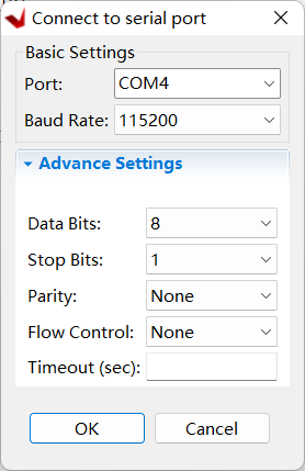
Connect to Serial Port
Run the lab7 application from the DDR3 memory.
- Right-click on lab7 from the Explorer View and select Run as > Launch Hardware (Single Application Debug).
- Follow the menu in the terminal emulator window and test transfers between various memories.
- Select option 4 in the menu to complete the execution.
- Close Vitis IDE and Vivado
- Turn OFF the power on the board.
Conclusion
This lab led you through adding a CDMA controller to the PS so that you can perform DMA transfers between various memories. You used the high-performance port so DMA could be done between the BRAM residing in the PL section and DDR3 connected to the PS. You verified the design functionality by creating an application and executing it from the DDR3 memory.