Vivado Design Flow
Objectives
After completing this lab, you will be able to:
- Create a Vivado project sourcing HDL model(s) and targeting the ZYNQ or Spartan devices located on the Boolean or PYNQ-Z2 boards.
- Use the provided Xilinx Design Constraint (XDC) file to constrain the pin locations.
- Simulate the design using the Vivado simulator.
- Synthesize and implement the design.
- Generate the bitstream.
- Configure ZYNQ and Spartan using the generated bitstream and verify the functionality.
In the instructions for the tutorial
The absolute path for the source code should only contain ascii characters. Deep path should also be avoided since the maximum supporting length of path for Windows is 260 characters.
{SOURCES} refers to .\source\{BOARDS}\. You can use the source files from the cloned repository’s source directory.
{TUTORIAL} refers to C:\vivado_tutorial\. It assumes that you will create the mentioned directory structure to carry out the labs of this tutorial.
{BOARDS} refers to target Boolean and PYNQ-Z2 boards.
Steps
Create a Vivado Project
Launch Vivado and create an empty project targeting the XC7S50CSGA324-1 (for Boolean) or XC7Z020CLG400-1 (for PYNQ-Z2), selecting Verilog as a target language. Use the provided lab1.v, and lab1_zynq.xdc (for PYNQ-Z2) and lab1_spartan.xdc (for Boolean) files from the .\sources\lab1\ directory.
- Open Vivado by selecting Start > Xilinx Design Tools > Vivado 2021.2.
- Click Create New Project to start the wizard. You will see Create A New Vivado Project dialog box. Click Next.
- Click the Browse button of the Project location field of the New Project form, browse to {TUTORIAL}, i.e. C:\vivado_tutorial, and click Select.
-
Enter lab1 in the Project name field. Make sure that the Create Project Subdirectory box is checked. Click Next.
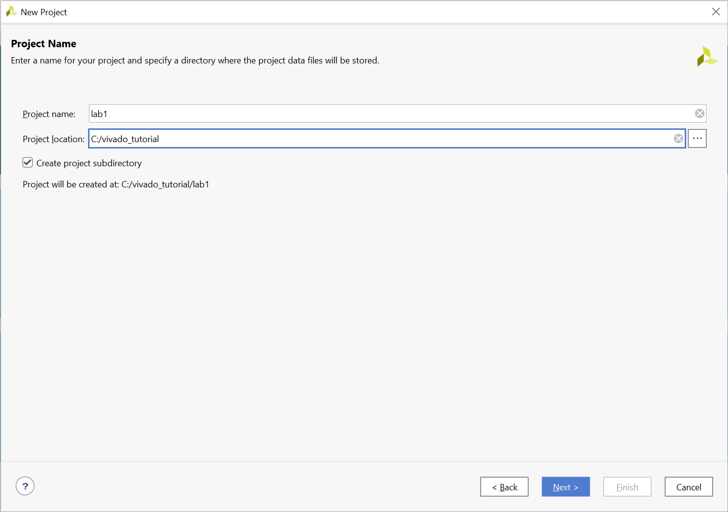
Project Name and Location entry
-
Select RTL Project option ONLY in the Project Type form, and click Next.
-
Using the drop-down buttons, select Verilog as the Target Language and Simulator Language in the Add Sources form.

Selecting Target and Simulator language
-
Click on the Blue Plus button, then click Add Files… and browse to the {sources}\{BOARD}\lab1 directory, select lab1.v, and click OK.

Adding source files
If it is not already checked, check Copy sources into project
-
Click Next to get to the Add Constraints form.
-
Click on the Blue Plus button, then click Add Files… and browse to the {SOURCES}\lab1 directory (if necessary), select lab1_pynq.xdc (for PYNQ-Z2) or lab1_boolean.xdc (for Boolean) and click OK (if necessary), and then click Next.
The Xilinx Design Constraints file assigns the physical IO locations on FPGA to the switches and LEDs located on the board. This information can be obtained either through the board’s schematic or the board’s user guide.
-
In the Default Part form, use the Parts option and various drop-down fields of the Filter section. Select the XC7Z020clg400-1(for PYNQ-Z2) or xc7s50csga-1 (for Boolean).
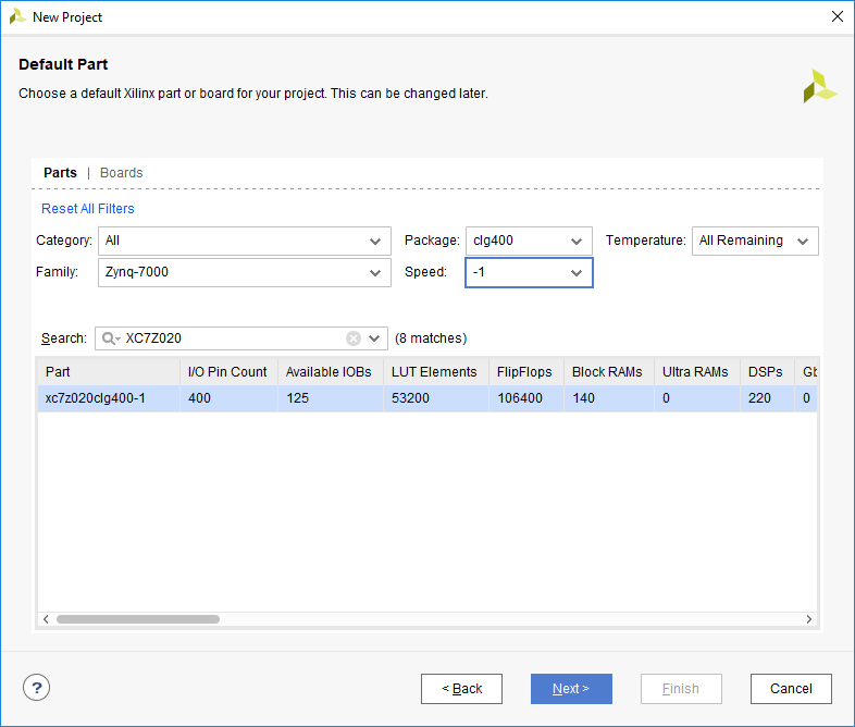
Part Selection for the PYNQ
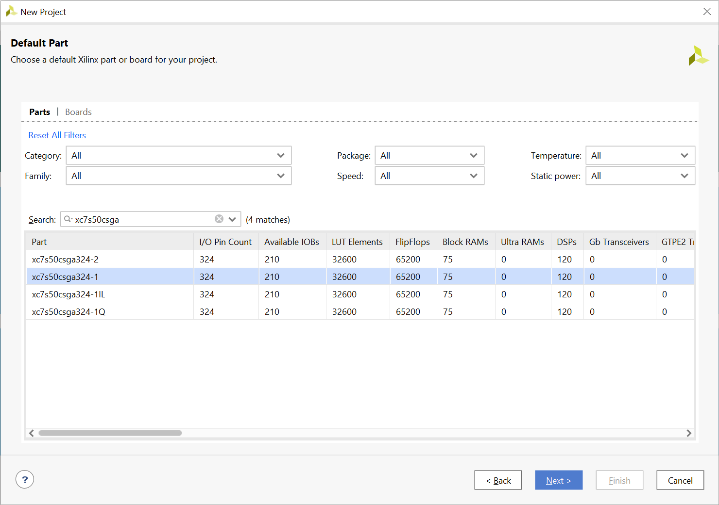
Part Selection for the Boolean
You may also select the Boards option,
tulembedded.comfor the PYNQ-Z2 board orRealDigital.orgfor the Boolean board under the Vendor filter and select the appropriate board. Notice that Boolean and PYNQ-Z2 may not be listed as they are not in the tools database. If not listed then you can download the board files for the desired boards from the respective board vendor webpage. -
Click Next.
- Click Finish to create the Vivado project.
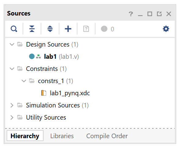
Use the Windows Explorer and look at the {TUTORIAL}\lab1 directory. You will find that the lab1.cache and lab1.srcs directories and the lab1.xpr (Vivado) project file have been created. The lab1.cache directory is a place holder for the Vivado program database. Two directories, constrs_1 and sources_1, are created under the lab1.srcs directory; deep down under them, the copied lab1_
lab1
│  lab1.xpr
│  struc.txt
│
├─lab1.cache
│  └─wt
│          project.wpc
│
├─lab1.hw
│      lab1.lpr
│
├─lab1.ip_user_files
├─lab1.sim
└─lab1.srcs
    ├─constrs_1
    │  └─imports
    │      └─lab1
    │              lab1_spartan.xdc
    │
    └─sources_1
        └─imports
            └─lab1
                    lab1.v
Open the lab1.v source and analyze the content.
-
In the Sources pane, double-click the lab1.v entry to open the file in text mode.

Opening the source file
-
Notice in the Verilog code that the first line defines the timescale directive for the simulator. Lines 2-4 are comment lines describing the module name and the purpose of the module.
-
Line 7 defines the beginning (marked with keyword module) and Line 17 defines the end of the module (marked with keyword endmodule).
-
Lines 8-9 defines the input and output ports whereas lines 12-15 defines the actual functionality.
Open the lab1_{BOARDS}.xdc source and analyze the content.
For PYNQ-Z2:
-
In the Sources pane, expand the Constraints folder and double-click the lab1_pynq.xdc entry to open the file in text mode.
Opening the Constraint File
-
Lines 5-8 define the pin locations for the input buttons and lines 13-16 define pin locations for output LEDs.
For Boolean
-
In the Sources pane, expand the Constraints folder and double-click the lab1_boolean.xdc entry to open the file in text mode.

-
Lines 17-20 define the pin locations for the input buttons and lines 10-13 define pin locations for output LEDs.
Perform RTL analysis on the source file.
Expand the Open Elaborated Design entry under the RTL Analysis tasks of the Flow Navigator pane and click on Schematic.
The model (design) will be elaborated and a logic view of the design is displayed.
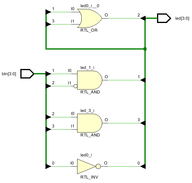
A Logic View of The Design
Simulate the Design using the Vivado Simulator
Add the lab1_tb.v testbench file.
-
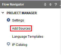
Click Add Sources under the Project Manager tasks of the Flow Navigator pane.
Add Sources
-
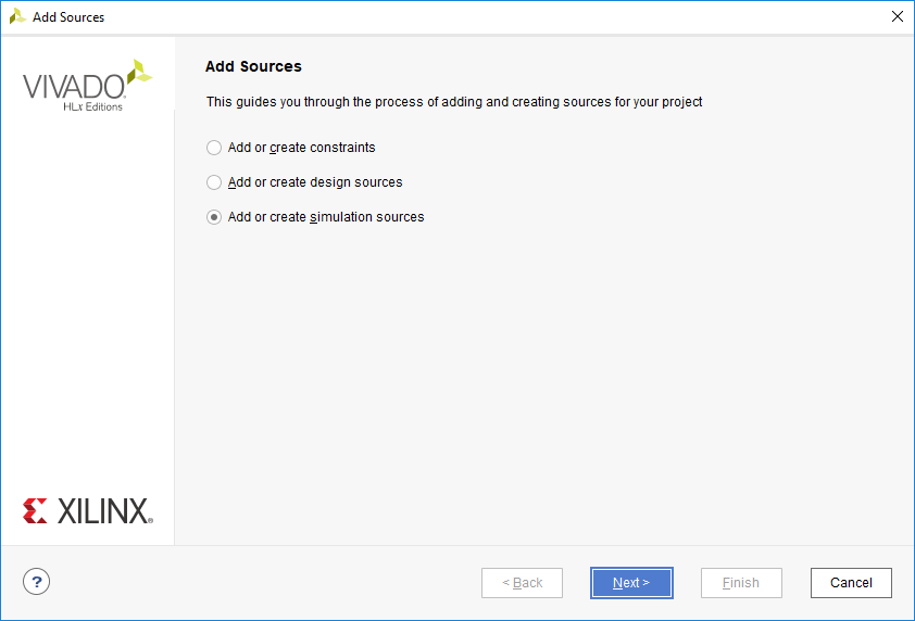
Select the Add or Create Simulation Sources option and click Next.
Selecting Simulation Sources option
-
In the Add Sources Files form, click the Blue Plus button and then then Add Files….
-
Browse to the {SOURCES}\lab1 folder and select lab1_tb.v and click OK.
-
Click Finish.
-
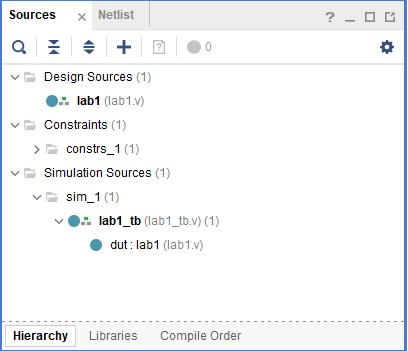
Select the Sources tab and expand the Simulation Sources group.
The lab1_tb.v file is added under the Simulation Sources group, and lab1.v is automatically placed in its hierarchy as a dut (device under test) instance.
Simulation Sources Hierarchy
-
Using the Windows Explorer, verify that the sim_1 directory is created at the same level as constrs_1 and sources_1 directories under the lab1.srcs directory, and that a copy of lab1_tb.v is placed under lab1.srcs > sim_1 > imports > lab1.
-
Double-click on the lab1_tb in the Sources pane to view its contents.

The self-checking test bench
The test bench defines the simulation step size and the resolution in line 1. The test bench module definition begins on line 5. Line 15 instantiates the DUT (device/module under test). Lines 17 through 25 define the same module functionality for the expected value computation. Lines 27 through 38 define the stimuli generation, and compare the expected output with what the DUT provides. Line 40 ends the test bench. The $display task will print the message in the simulator console window when the simulation is run.
Simulate the design for 200 ns using the Vivado simulator.
-
Select Settings under the Project Manager tasks of the Flow Navigator pane.
A Settings form will appear showing the Simulation properties form.
-
Select the Simulation tab, and set the Simulation Run Time value to 200 ns and click OK.
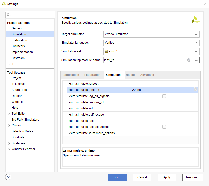
Setting simulation run time
-
Click on Simulation > Run Simulation > Run Behavioral Simulation under the Project Manager tasks of the Flow Navigator pane.
The testbench and source files will be compiled and the Vivado simulator will be run (assuming no errors). You will see a simulator output like the one shown below.
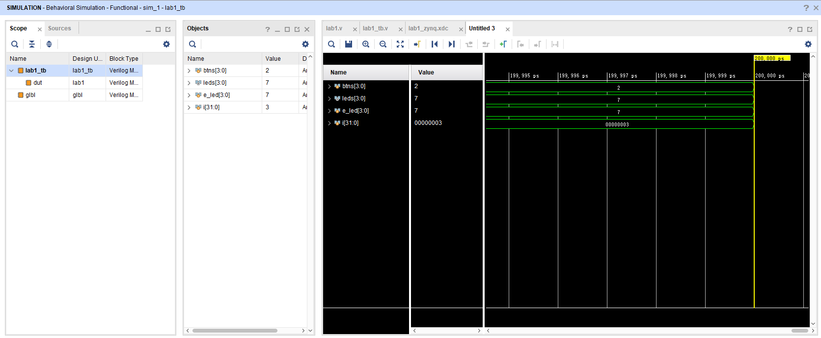
Simulator output
You will see four main views: (i) Scopes, where the testbench hierarchy as well as glbl instances are displayed, (ii) Objects, where top-level signals are displayed, (iii) the waveform window, and (iv) Tcl Console where the simulation activities are displayed. Notice that since the testbench used is self-checking, the results are displayed as the simulation is run.
Notice that the lab1.sim directory is created under the lab1 directory, along with several lower-level directories.
//Directory structure after running behavioral simulation
lab1.sim
└─sim_1
   └─behav
      └─xsim
            │  compile.bat
            │  compile.log
            │  elaborate.bat
            │  elaborate.log
            │  glbl.v
            │  lab1_tb.tcl
            │  lab1_tb_behav.wdb
            │  lab1_tb_vlog.prj
            │  simulate.bat
            │  simulate.log
            │  xelab.pb
            │  xsim.ini
            │  xvlog.log
            │  xvlog.pb
            │
            └─xsim.dir
               ├─lab1_tb_behav
               │  │  Compile_Options.txt
               │  │  TempBreakPointFile.txt
               │  │  xsim.dbg
               │  │  xsim.mem
               │  │  xsim.reloc
               │  │  xsim.rlx
               │  │  xsim.rtti
               │  │  xsim.svtype
               │  │  xsim.type
               │  │  xsim.xdbg
               │  │  xsimcrash.log
               │  │  xsimk.exe
               │  │  xsimkernel.log
               │  │
               │  └─obj
               │          xsim_0.win64.obj
               │          xsim_1.c
               │          xsim_1.win64.obj
               │
               └─xil_defaultlib
                        glbl.sdb
                        lab1.sdb
                        lab1_tb.sdb
                        xil_defaultlib.rlx
You will see several buttons next to the waveform window which can be used for the specific purpose as listed in the table below.

Various buttons available to view the waveform
-
Click on the Zoom Fit button (
 ) to see the entire waveform.
Notice that the output changes when the input changes.
You can also float the simulation waveform window by clicking on the Float button (
 ) on the upper right hand side of the view. This will allow you to have a wider window to view the simulation waveforms. To reintegrate the floating window back into the GUI, simply click on the Dock Window button (
 ).
).
Change display format if desired.
Select i[31:0] in the waveform window, right-click, select Radix, and then select Unsigned Decimal to view the for-loop index in an unsigned integer form. Similarly, change the radix of btn[3:0] to Hexadecimal. Leave the leds[3:0] and e_led[3:0] radix to binary as we want to see each output bit.
Add more signals to monitor the lower-level signals and continue to run the simulation for 500 ns.
-
Expand the lab1_tb instance, if necessary, in the Scopes window and select the dut instance.
The btn[3:0] and led[3:0] signals will be displayed in the Objects window.
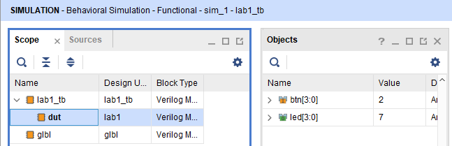
Selecting Lower-Level Signals
-
Select btn[3:0] and led[3:0] and drag them into the waveform window to monitor those lower-level signals.
- On the simulator tool buttons ribbon bar
 , type 500 over in the simulation run time field, click on the drop-down button of the units field and select ns since we want to run for 500 ns (total of 700 ns), and click on the (
 ) button. The simulation will run for an additional 500 ns.
 -
Click on the Zoom Fit button and observe the output.
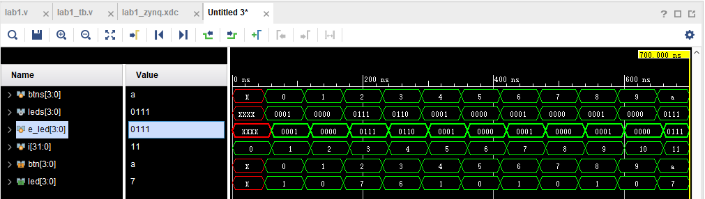
Running simulation for additional 500 ns
Observe the Tcl Console window and see the output is being displayed as the testbench uses the $display task.
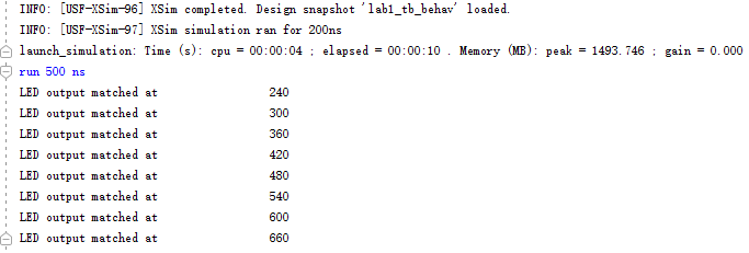
Tcl Console output after running the simulation for additional 500 ns
-
Close the simulator by selecting File > Close Simulation.
- Click OK and then click Discard to close it without saving the waveform.
Synthesize the Design and Analyze the Project Summary Output.
-
Click on Run Synthesis under the SYNTHESIS tasks of the Flow Navigator pane.
The synthesis process will be run on the lab1.v file (and all its hierarchical files if they exist). When the process is completed a Synthesis Completed dialog box with three options will be displayed.
-
Select the Open Synthesized Design option and click OK as we want to look at the synthesis output before progressing to the implementation stage.
Click Yes to close the elaborated design if the dialog box is displayed.
-
Select the Project Summary tab and understand the various windows.
If you don’t see the Project Summary tab then select Window > Project Summary or click the Project Summary icon
 .
.
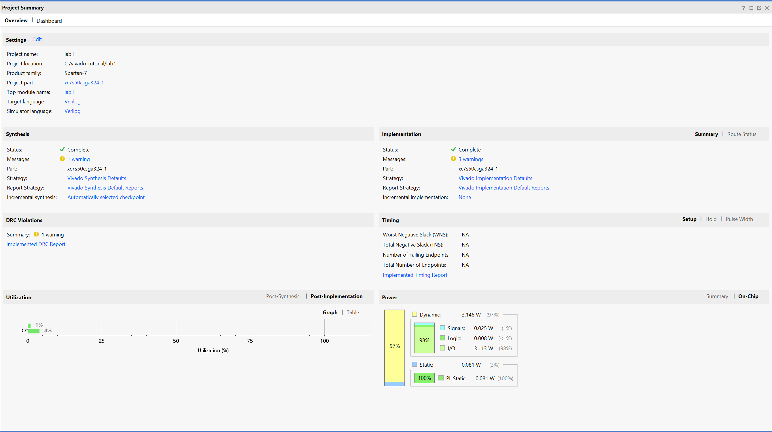
Project Summary view
Click on the various links to see what information they provide and which allows you to change the synthesis settings.
-
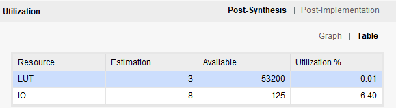
Click on the Table tab in the Project Summary tab.
Notice that there are an estimated 3 LUTs and 8 IOs (4 input and 4 output) that are used.
Resource utilization estimation summary
-
In The Flow Navigator, under Synthesis (expand Open Synthesized Design if necessary), click on Schematic to view the synthesized design in a schematic view.
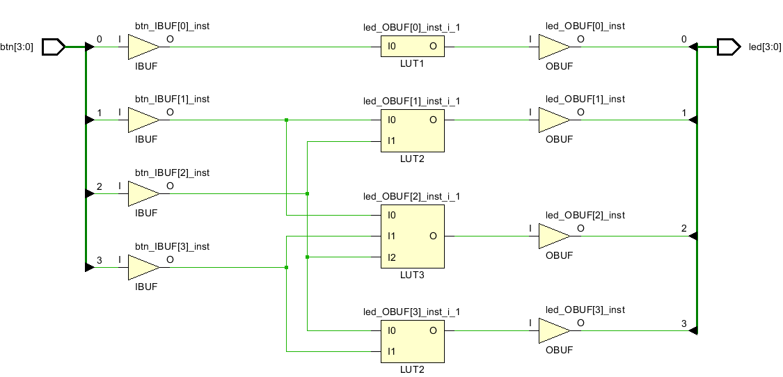
Synthesized design’s schematic view
Notice that IBUFs and OBUFs are automatically instantiated (added) to the design as the input and output are buffered. The logical gates are implemented in LUTs (1 input is listed as LUT1, 2 input is listed as LUT2, and 3 input is listed as LUT3). Four gates in RTL analysis output are mapped onto 3 LUTs in the synthesized output.
Using Windows Explorer, verify that lab1.runs directory is created under lab1. Under the runs directory, synth_1 directory is created which holds several files related to synthesis.
//Directory structure after synthesizing the design
lab1.runs
├─.jobs
└─synth_1
    └─.Xil
Implement the Design
-
Click on Run Implementation under the Implementation tasks of the Flow Navigator pane.
The implementation process will be run on the synthesized design. When the process is completed an Implementation Completed dialog box with three options will be displayed. You can choose to use how many jobs you want to implement this design. In general, more jobs consumes more computing resources and less runtime

Select the threads(jobs) you want to use for implementation
-
Select Open implemented design and click OK as we want to look at the implemented design in a Device view tab.
- Click Yes, if prompted, to close the synthesized design. The implemented design will be opened.
-
In the Netlist pane, select one of the nets (e.g. led_OBUF[3]) and notice that the net displayed in the X1Y2 clock region in the Device view tab (you may have to zoom in to see it).
-
If it is not selected, click the Routing Resources icon
 to show routing resources.
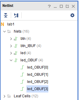
Viewing implemented design
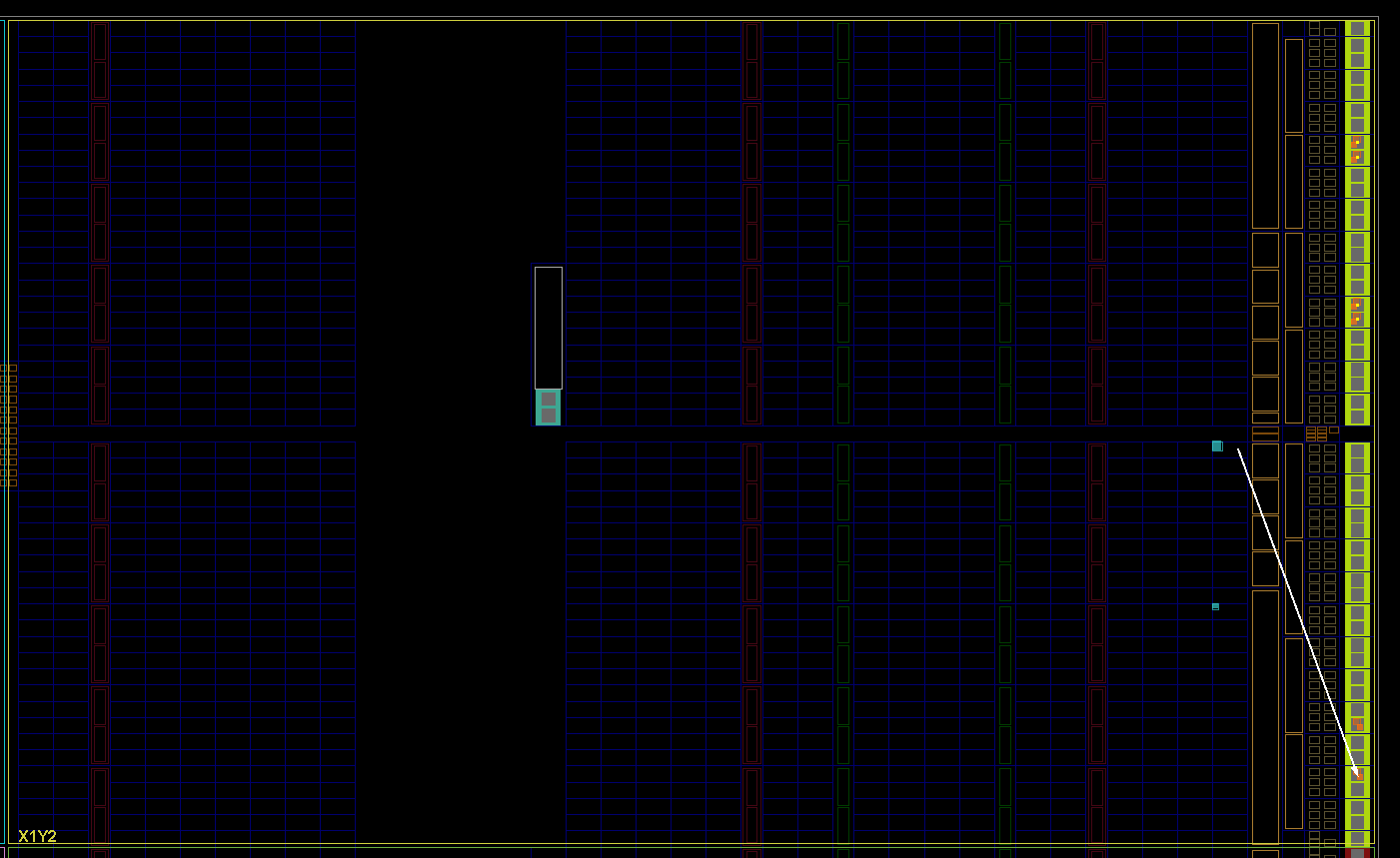
Selecting a net
-
Close the implemented design view by selecting File > Close Implemented Design, and select the Project Summary tab (you may have to change to the Default Layout view) and observe the results.
-
Select the Post-Implementation tab.
Notice that the actual resource utilization is 3 LUTs and 8 IOs. Also, it indicates that no timing constraints were defined for this design (since the design is combinational).
Implementation results for the Boolean
Using the Windows Explorer, verify that impl_1 directory is created at the same level as synth_1 under the lab1.runs directory. The impl_1 directory contains several files including the implementation report files.
-
In Vivado, select the Reports tab in the bottom panel (if not visible, click Window in the menu bar and select Reports), and double-click on the Utilization Report entry under the Place Design section. The report will be displayed in the auxiliary view pane showing resource utilization. Note that since the design is combinatorial, no registers are used.
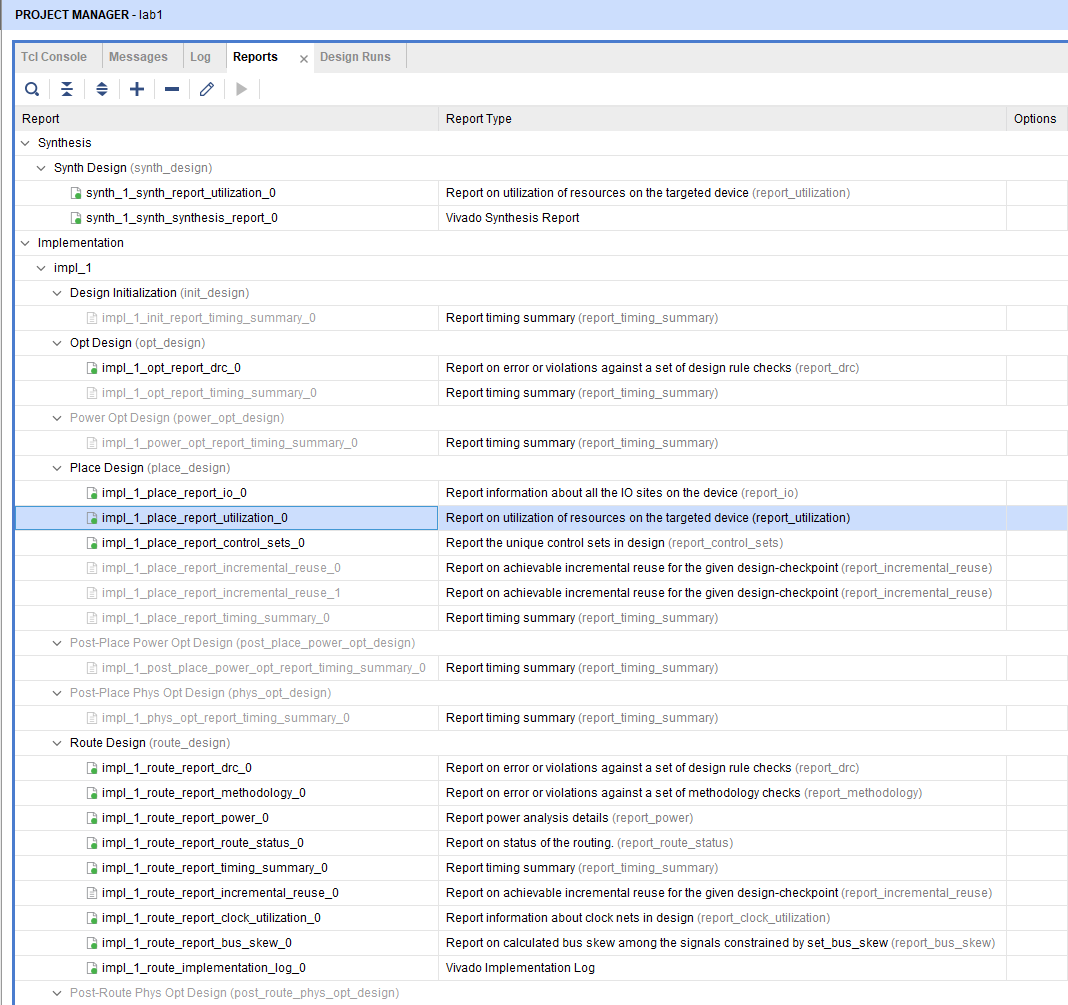
Available reports to view
Perform Timing Simulation
-
Select Run Simulation > Run Post-Implementation Timing Simulation process under the Simulation tasks of the Flow Navigator pane.
The Vivado simulator will be launched using the implemented design and lab1_tb as the top-level module.
Using the Windows Explorer, verify that timing directory is created under the lab1.sim > sim_1 > impl directory. The timing directory contains generated files to run the timing simulation.
-
Click on the Zoom Fit button to see the waveform window from 0 to 200 ns.
-
Right-click at 50 ns (where the btns input is set to 0000b) and select Markers > Add Marker.
-
Similarly, right-click and add a marker at around 58.000 ns where the leds changes.
-
You can also add a marker by clicking on the Add Marker button (
 ). Click on the Add Marker button and left-click at around 60 ns where e_led changes.
Timing simulation output
Notice that we monitored the expected led output at 10 ns after the input is changed (see the testbench) whereas the actual delay is about 8 to 9.7 ns (depending on the board).
-
Close the simulator by selecting File > Close Simulation without saving any changes.
Generate the Bitstream and Verify Functionality
Connect the board and power it ON. Generate the bitstream, open a hardware manager session, and program the FPGA.
-
Make sure that the Micro-USB cable is connected to the JTAG PROG connector.
-
The Boolean and PYNQ-Z2 can be powered through USB power via the JTAG PROG.
Make sure that the board is set to use USB power.
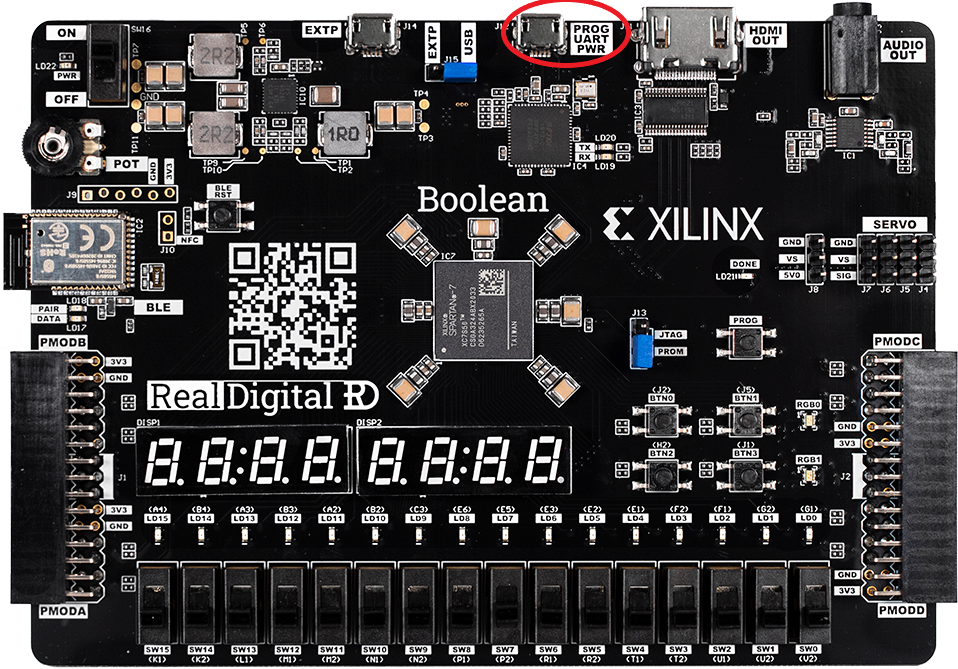
Board connection for the Boolean

Board Connection for the PYNQ-Z2
-
Power ON the board.
-
Click on the Generate Bitstream entry under the PROGRAM AND DEBUG tasks of the Flow Navigator pane.
The bitstream generation process will be run on the implemented design. When the process is completed a Bitstream Generation Completed dialog box with three options will be displayed.
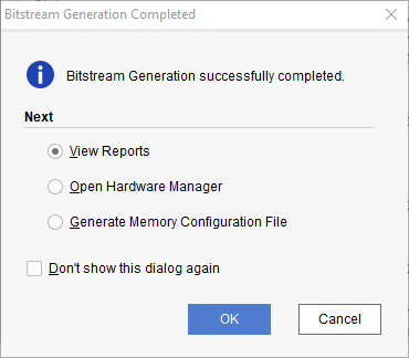
Bitstream Generation
This process will have generated a lab1.bit file under the lab1.runs > impl_1 directory.
-
Select the Open Hardware Manager option and click OK.
The Hardware Manager window will open indicating “unconnected” status.
-
Click on the Open target link.

Opening new Hardware Target
-
From the dropdown menu, click Auto Connect.
For PYNQ-Z2:
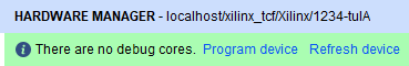
The Hardware Session status changes from Unconnected to the server name and the device is highlighted. Also notice that the Status indicates that it is not programmed.
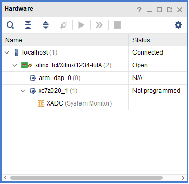
Opened hardware manager session
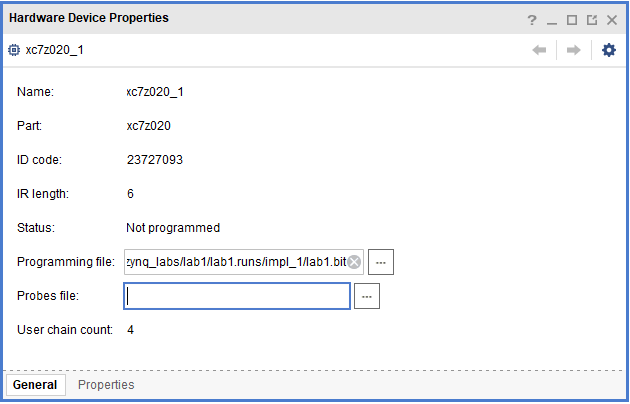
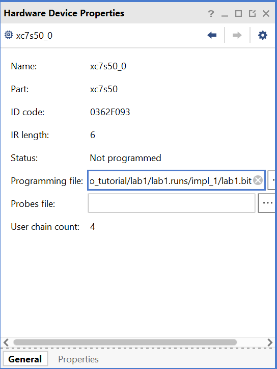
Select the device and verify that the lab1.bit is selected as the programming file in the General tab.
Programming File
For Boolean:
The Hardware Session status changes from Unconnected to the server name and the device is highlighted. Also notice that the Status indicates that it is not programmed.

Opened hardware manager session
Select the device and verify that the lab1.bit is selected as the programming file in the General tab.
-
Click on the Program device link in the green information bar to program the target FPGA device. Another way is to right click on the device and select Program Device.
Selecting to program the FPGA
-
Click Program to program the FPGA.
The DONE LED will lit when the device is programmed. You may see some other LEDs lit depending on switch positions.
-
Verify the functionality by flipping the switches and observing the output on the LEDs (Refer to the earlier logic diagram).
-
When satisfied, close the hardware manager session by selecting File > Close Hardware Manager.
-
Click OK to close the session.
-
Power OFF the board.
-
Close the Vivado program by selecting File > Exit and click OK.
Conclusion
The Vivado software tool can be used to perform a complete HDL based design flow. The project was created using the supplied source files (HDL model and user constraint file). A behavioral simulation using the provided testbench was done to verify the model functionality. The model was then synthesized, implemented, and a bitstream was generated. The timing simulation was run on the implemented design using the same testbench. The functionality was verified in hardware using the generated bitstream.
Copyright© 2023, Advanced Micro Devices, Inc.