Synthesizing a RTL Design
Objectives
After completing this lab, you will be able to:
-
Use the provided Xilinx Design Constraint (XDC) file to constrain the timing of the circuit.
-
Elaborate on the design and understand the output.
-
Synthesize the design with the provided basic timing constraints.
-
Analyze the output of the synthesized design.
-
Change the synthesis settings and see their effects on the generated output.
-
Write a checkpoint after the synthesis so the results can be analyzed after re-loading it.
Procedure
This lab is broken into steps that consist of general overview statements providing information on the detailed instructions that follow. Follow these detailed instructions to progress through the lab.
Design Description
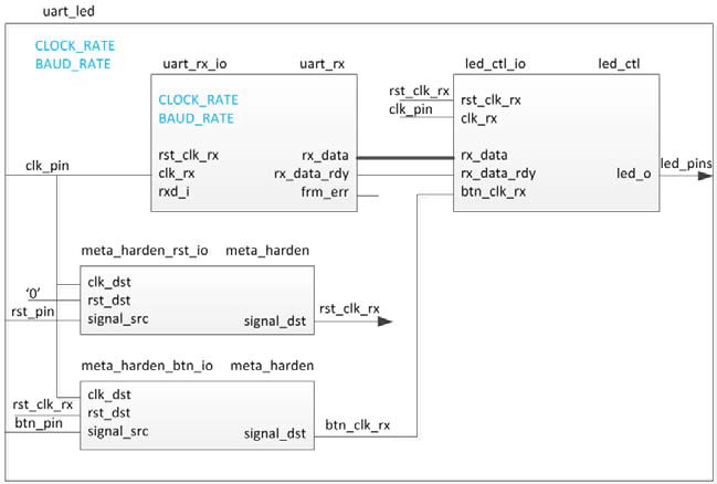
The design consists of a uart receiver receiving the input typed on a keyboard and displaying the binary equivalent of the typed character on the 8 LEDs. When a push button is pressed, the lower and upper nibbles are swapped. The block diagram is as shown in the following figure.
The Completed Design
General Flow
flowchart
	1(Step 1 : Create a Vivado Project)-->2(Step 2: Elaborate the Design)-->3(Step 3: Synthesize the Design)-->4(Step 4: Read the Check points)
In the instructions for the tutorial
The absolute path for the source code should only contain ascii characters. Deep path should also be avoided since the maximum supporting length of path for Windows is 260 characters.
{SOURCES} refers to .\source\{BOARD}\. You can use the source files from the cloned repository’s source directory.
{TUTORIAL} refers to C:\vivado_tutorial\. It assumes that you will create the mentioned directory structure to carry out the labs of this tutorial.
{BOARD} refers to target Boolean and Z2 boards.
Step 1 Create a Vivado Project
Launch Vivado and create an empty project targeting the XC7S50CSGA324-1(for Boolean) or XC7Z020CLG400-1 (PYNQ-Z2) board, selecting Verilog as a target language. Use the provided Verilog source files, uart_led_pins_{board}.xdc and uart_led_timing.xdc files from the {SOURCES}\lab2 directory.
-
Open Vivado by selecting Start > All Programs > Xilinx Design Tools > Vivado 2021.2.
-
Click Create New Project to start the wizard. You will see Create A New Vivado Project dialog box. Click Next.
-
Click the Browse button of the Project location field of the New Project form, browse to {TUTORIAL}, and click Select.
-
Enter lab2 in the Project name field. Make sure that the Create Project Subdirectory box is checked. Click Next.
-
Select RTL Project option in the Project Type form, and click Next.

Create a new project
-
Using the drop-down buttons, select Verilog as the Target Language and Simulator Language in the Add Sources form.
-
Click on the Green Plus button, then the Add Files… button and browse to the {SOURCES}\{BOARD}\lab2 directory, select all the Verilog files (led_ctl.v, meta_harden.v, uart_baud_gen.v, uart_led.v, uart_rx.v, and uart_rx_ctl.v), click OK, and then click Next to get to the Add Existing IP form.
-
Since we do not have any IP to add, click Next to get to the Add Constraints form.
-
Click on the Blue Plus button, then Add Files… and browse to the {sources}\lab2 directory (if necessary), select uart_led_timing.xdc and click Open.
-
Click Next. This Xilinx Design Constraints file assigns the basic timing constraints (period, input delay, and output delay) to the design.
-
In the Default Part form, using the Parts option and various drop-down fields of the Filter section, select XC7S50CSGA324-1(for Boolean) or XC7Z020CLG400-1(PYNQ-Z2).
-
Click Next.
-
Click Finish to create the Vivado project.
(If you are using PYNQ-Z2)
-
Copy the tcl script
ps_init.tclfrom {SOURCES}/pynq-z2/lab2 to {TUTORIAL}/lab2.In the Tcl Shell window enter the following command to change to the lab directory and hit Enter.cd {TUTORIAL}/lab2 -
Generate the PS design by executing the provided Tcl script.
source ps_init.tcl
Please check if the path in the tcl script is correct or not.
Analyze the design source files hierarchy (Taking Boolean as an example).
-
In the Sources pane, expand the uart_led entry and notice hierarchy of the lower-level modules.

Opening the source file (Boolean as example)
- Double-click on the uart_led entry to view its content. Notice in the Verilog code, the BAUD_RATE and CLOCK_RATE parameters are defined to be 115200 and 125M Hz(PYNQ-Z2) or 100 MHz(Boolean) respectively as shown in the design diagram. Also notice that the lower level modules are instantiated. The meta_harden modules are used to synchronize the asynchronous reset and push-button inputs.
-
Expand uart_rx_i0 instance to see its hierarchy. This module uses the baud rate generator and a finite state machine. The rxd_pin is sampled at a x16 the baud rate.
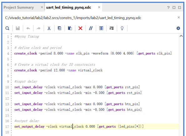
Open the uart_led_timing.xdc source and analyze the content.
-
In the Sources pane, expand the Constraints folder and double-click the uart_led_timing_{BOARD}.xdc entry to open the file in text mode.
Timing constraints
Line 3 creates the period constraint of 10 ns with a duty cycle of 50%. Line 6 creates a virtual clock of 12 ns. This clock can be viewed as the upstream device is generating its output with respect to its clock and outputs data with respect to it. The rxd_pin is constrained with respect to the design clock (lines 9, and 10) whereas the btn_pin is constrained with respect to the upstream clock (lines 12, 13). The led_pins are constrained with respect to the upstream clock as the downstream device may be using it.
Step 2 Elaborate the Design
Elaborate and perform the RTL analysis on the source file.
-
Expand the Open Elaborated Design entry under the RTL Analysis tasks of the Flow Navigator pane and click on Schematic. The model (design) will be elaborated and a logical view of the design is displayed.

A logic view of the design
A logic view of the design
You will see four components at the top-level, 2 instances of meta_harden, one instance of uart_rx, and one instance of led_ctl.
- To see where the uart_rx_i0 gets generated, right-click on the uart_rx_i0 instance and select Go To Source and see that line 84 in the source code is generating it.
-
Double-click on the uart_rx_i0 instance in the schematic diagram to see the underlying components.

Lower level components of the uart_rx_i0 module
- Click on Report Noise under the Open Elaborated Design entry of the RTL Analysis tasks of the Flow Navigator pane.
-
Click OK to generate the report named ssn_1.

Noise report
-
View the ssn_1 report and observe the unplaced ports, Summary, and I/O Bank Details are highlighted in red because the pin assignments were not done. Note that only output pins are reported as the noise analysis is done on the output pins.
-
Click on Add Sources under the Project Navigator, select Add or Create Constraints option and click Next.
-
Click on the Blue Plus button, then the Add Files… button and browse to the {sources}\lab2 directory, select the uart_led_pins_{BOARDS}.xdc file (depending on the target board), click OK, and then click Finish to add the pins location constraints.
Notice that the sources are modified and the tools detect it, showing a warning status bar to reload the design.

- Click on the Reload link. The constraints will be processed.
- Click on Report Noise and click OK to generate the report named ssn_1. Observe that this time it does not show any errors (no red).
Step 3 Synthesize the Design
Synthesize the design with the Vivado synthesis tool and analyze the Project Summary output.
-
Click on Run Synthesis under the Synthesis tasks of the Flow Navigator pane.
The synthesis process will be run on the uart_led.v and all its hierarchical files. When the process is completed a Synthesis Completed dialog box with three options will be displayed.
-
Select the Open Synthesized Design option and click OK as we want to look at the synthesis output.
Click Yes to close the elaborated design if the dialog box is displayed.
-
Select the Project Summary tab
If you don’t see the Project Summary tab then select Layout > Default Layout .
-
Click on the Table tab in the Project Summary tab and fill out the following information.
Question 1
Look through the table and find the number used of each of the following:
Resources Estimation FF LUT I/O BUFG -
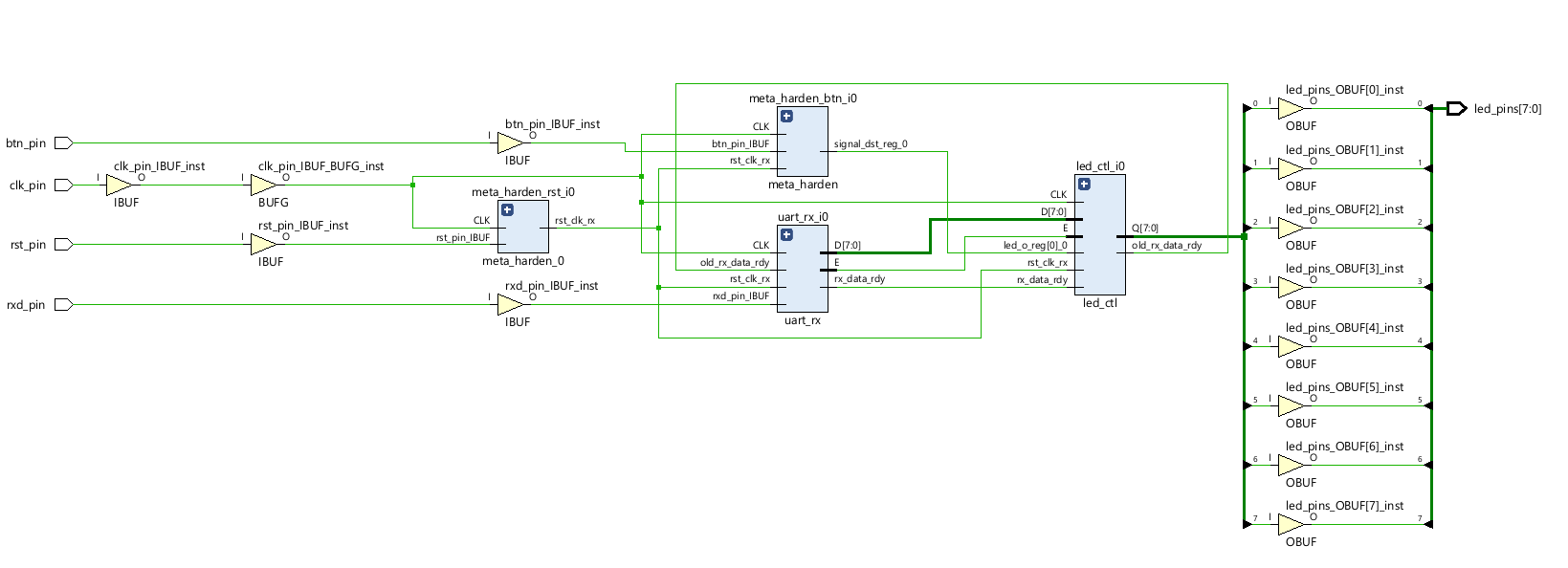
Click on Schematic under the Open Synthesized Design tasks of Synthesis tasks of the Flow Navigator pane to view the synthesized design in a schematic view.
Synthesized design’s schematic view
Notice that IBUF and OBUF are automatically instantiated (added) to the design as the input and output are buffered. There are still four lower level modules instantiated.
-
Double-click on the uart_rx_i0 instance in the schematic view to see the underlying instances.
-
Select the uart_baud_gen_rx_i0 instance, right-click, and select Go To Source.
Notice that the line instantiated uart_rx_i0 is highlighted. Also notice that the CLOCK_RATE and BAUD_RATE parameters are passed to the module being called.
-
Go back to the schematic, double-click on the meta_harden_rxd_io instance to see how the synchronization circuit is implemented using two FFs. This synchronization is necessary to reduce the likelihood of metastability.
-
Click on the (
 ) in the schematic view to go back to its parent block.
Analyze the timing report
- Click on Report Timing Summary under the Synthesized Design tasks of the Flow Navigator pane.
-
Click OK to generate the Timing_1 report.
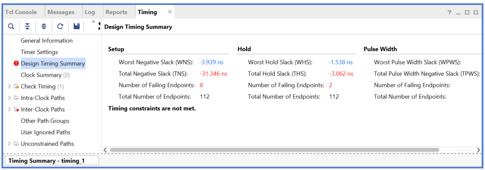
Timing report for the Boolean
Notice that the Design Timing Summary and Inter-Clock and Intra-Clock Paths entry in the left pane is highlighted in red indicating timing violations. In the right pane, the information is grouped in Setup, Hold, and Width columns.
Under the Setup column Worst Negative Slack (WNS) is linked indicating that clicking on it can give us insight on how the failing path has formed. The Total Negative Slack (TNS) is highlighted in red indicating the total amount of violations in the design and the Number of Failing Endpoints indicate total number of failing paths.
-
Click on the WNS link and see the 8 failing paths.

The 8 failing paths for the Boolean
-
Double-click on the Path 23 to see how the path is made.

Worst failing path for the Boolean
Note that this is an estimate only. The nets are specified as unplaced and have all been allocated default values (0.800 ns). No actual routing delays are considered.
Generate the utilization and power reports.
-
Click Report Utilization under the Synthesized Design, and click OK to generate the utilization report.
Utilization report for the Boolean
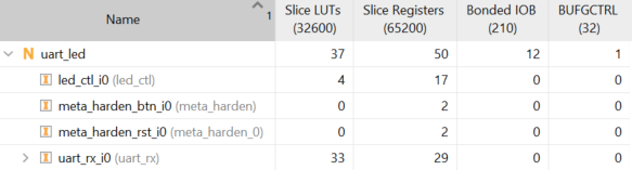
Question 2
Look through the table and find the number used of each of the following:
Resources Estimation FF LUT I/O BUFG -
Select Slice LUTs entry in the left pane and see the utilization by lower-level instances. You can expand the instances in the right pane to see the complete hierarchy utilization.

Utilization of lower-level modules for the Boolean
-
Click Report Power under the Synthesized Design, and click OK to generate the estimated power consumption report using default values. Note that this is just an estimate as no simulation run data was provided and no accurate activity rate, or environment information was entered.
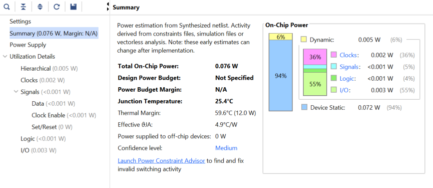
Question 3 From the power report, find the % power consumption used by each of the following:
| Categories | Partition |
|---|---|
| FF | % |
| LUT | % |
| I/O | % |
| BUFG | % |
You can move the mouse on the boxes which do not show the percentage to see the consumption.
Write the checkpoint in order to analyze the results without going through the actual synthesis process.
- Select File > Checkpoint > Write to save the processed design so it can be opened later for further analysis.
-
A dialog box will appear showing the default name of the file in the current project directory.
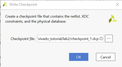
Wiring Checkpoint
- Click OK
Change the synthesis settings to flatten the design. Re-synthesize the design and analyze the results.
- Click on the Settings under the Project Manager, and select Synthesis.
-
Click on the flatten_hierarchy drop-down button and select full to flatten the design.

Selecting flatten hierarchy option
-
Click OK.
-
A Create New Run dialog box will appear asking you whether you want to create a new run since the settings have been changed.

Create New Run dialog box
-
Click Yes
-
Change the name from synth_1_copy_1 to synth_flatten and click OK.
-
Click Run Synthesis to synthesize the design.
-
Click OK to open the synthesized design when synthesis process is completed.
-
Click on Schematic under the Open Synthesized Design tasks of Synthesis tasks of the Flow Navigator pane to view the synthesized design in a schematic view. Notice that the design is completely flattened.
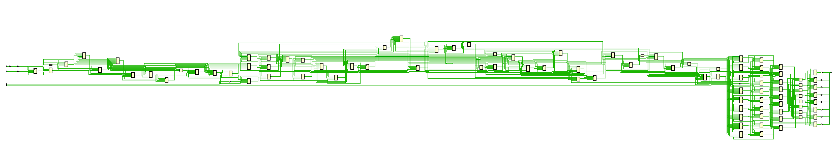 Flattened design
- Click on Report Utilization and observe that the hierarchical utilization is no longer available. Also note that the number of Slice Registers is 37.
Write the checkpoint in order to analyze the results without going through the actual synthesis process.
-
Select File > Checkpoint > Write to save the processed design so it can be opened later for further analysis.
-
A dialog box will appear showing the default name of the file in the current project directory.
-
Click OK.
Step 4 Read the Checkpoints
Read the previously saved checkpoint (checkpoint_1) in order to analyze the results without going through the actual synthesis process.
-
Launch Vivado and select *File > Checkpoint > Open ** at the *Getting Started Screen.
-
Browse to {TUTORIAL}/lab2 and select uart_led.dcp or system_wrapper.dcp
-
Click OK
-
If the schematic isn’t open by default, in the netlist tab, select the top-level instance, uart_led/system_wrapper, right-click and select Schematic.
You will see the hierarchical blocks. You can double-click on any of the first-level block and see the underlying blocks. You can also select any lower-level block in the netlist tab, right-click and select Schematic to see the corresponding level design.
-
In the netlist tab, select the top-level instance, uart_led, right-click and select Show Hierarchy.
You will see how the blocks are hierarchically connected.
-
Select Reports > Timing > Report Timing Summary and click OK to see the report you saw previously.
-
Select Reports > Report Utilization and click OK to see the utilization report you saw previously.
-
Select File > Open Checkpoint, browse to {TUTORIAL}/lab2 and select uart_led.dcp or system_wrapper.dcp.
-
Click No to keep the Checkpoint_1 open.
This will invoke second Vivado GUI.
-
If the schematic isn’t open by default, in the netlist tab, select the top-level instance, uart_led, right-click and select Schematic. You will see the flattened design.
-
You can generate the desired reports on this checkpoint as you wish.
-
Close the Vivado program by selecting File > Exit and click OK.
Conclusion
In this lab you applied the timing constraints and synthesized the design. You viewed various post-synthesis reports. You wrote checkpoints and read it back to perform the analysis you were doing during the design flow. You saw the effect of changing synthesis settings.
Copyright© 2023, Advanced Micro Devices, Inc.