Xilinx Design Constraints
Introduction
In this lab you will use the uart_led design that was introduced in the previous labs. You will start the project with I/O Planning type, enter pin locations, and export it to the rtl. You will then create the timing constraints and perform the timing analysis
Objectives
After completing this lab, you will be able to:
- Create a I/O Planning project.
- Enter the pin locations and IO standards via Device view, Package Pins tab, and Tcl commands.
- Create Period, Input Setup, and Output Setup delays.
- Perform timing analysis.
Design Description
The design consists of a uart receiver receiving the input typed on a keyboard and displaying the binary equivalent of the typed character on the 8 LEDs. When a push button is pressed, the lower and upper nibbles are swapped. If you are using a PYNQ-Z2 development board, please make sure that you have a blank microSD card with FAT32 file system.
For PYNQ-Z2:
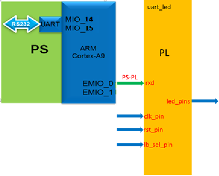
In this design we will use board’s USB-UART which is controlled by the Zynq’s ARM Cortex-A9 processor. Our PL design needs access to this USB-UART. First thing we will do is to create a processing system design which will put the USB-UART connections in a simple GPIO-style and make it available to the PL section.
The provided design places the UART (RX) pin of the PS (processing system) on the Cortex-A9 in a simple GPIO mode to allow the UART to be connected (passed through) to the Programmable Logic. The processor samples the RX signal and sends it to the EMIO channel 0 which is connected to Rx input of the HDL module provided in the Static directory. This is done through a software application which has been built on the booting image located in {SOURCES}/pynq-z2/BOOT.BIN
For Boolean:
Boolean board will be using the on-board UART port to implement such function, without configuring the PS side.

The Complete Design on PL
The Complete System on PYNQ-Z2
General Flow
flowchart TD
1:[Step 1: Create a Vivado I/O Planning Project] --> 2:[Step 2: Assign Various Pins and Source Files] --> 3:[Step 3: Synthesize and Enter Timing Constraints] --> 4:[Step 4:Implement and Perform Timing Analysis] --> 5:[Optional Step 5: Generate Bitstream and Verify]
Instructions for the tutorial
The absolute path for the source code should only contain ascii characters. Deep path should also be avoided since the maximum supporting length of path for Windows is 260 characters.
{SOURCES} refers to .\source\{BOARD}\Labn. You can use the source files from the cloned repository’s source directory
{TUTORIAL} refers to C:\vivado_tutorial\. It assumes that you will create the mentioned directory structure to carry out the labs of this tutorial
{BOARD} refers to target Boolean and Z2 boards.
Steps
Step 1 Create a Vivado I/O Planning Project
For PYNQ-Z2:
Launch Vivado and create a project targeting the XC7Z020clg400-1 device, and use the provided tcl script file (ps7_create_pynq.tcl) to generate the block design for the PS subsystem. Also, add the Verilog HDL files, uart_led_pins_pynq.xdc and uart_led_timing_pynq.xdc files from the {SOURCES}\{BOARD}\lab5 directory.
For Boolean:
Launch Vivado and create a project targeting XC7S50CSGA324-1 parts, and using the Verilog HDL. Use the provided Verilog source files and XDC files from the {SOURCES}\{BOARD}\lab5\ directory.
-
Open Vivado by selecting Start > Xilinx Design Tools > Vivado 2021.2.
-
Click Create New Project to start the wizard. You will see Create A New Vivado Project dialog box. Click Next.
-
Click the Browse button of the Project location field of the New Project form, browse to {TUTORIAL}, and click Select.
-
Enter lab5 in the Project name field. Make sure that the Create Project Subdirectory box is checked. Click Next.
-
Select the I/O Planning Project option in the Project Type form, and click Next.
-
Select Do not import I/O ports at this time, and click Next.
-
In the Default Part form, use the Parts option and various drop-down fields of the Filter section, select the XC7Z020clg400-1 part (for PYNQ-Z2) or XC7S50CSGA324-1 part(for Boolean).
-
Click Next.
-
Click Finish to create the Vivado project.
The device view window and package pins tab will be displayed.
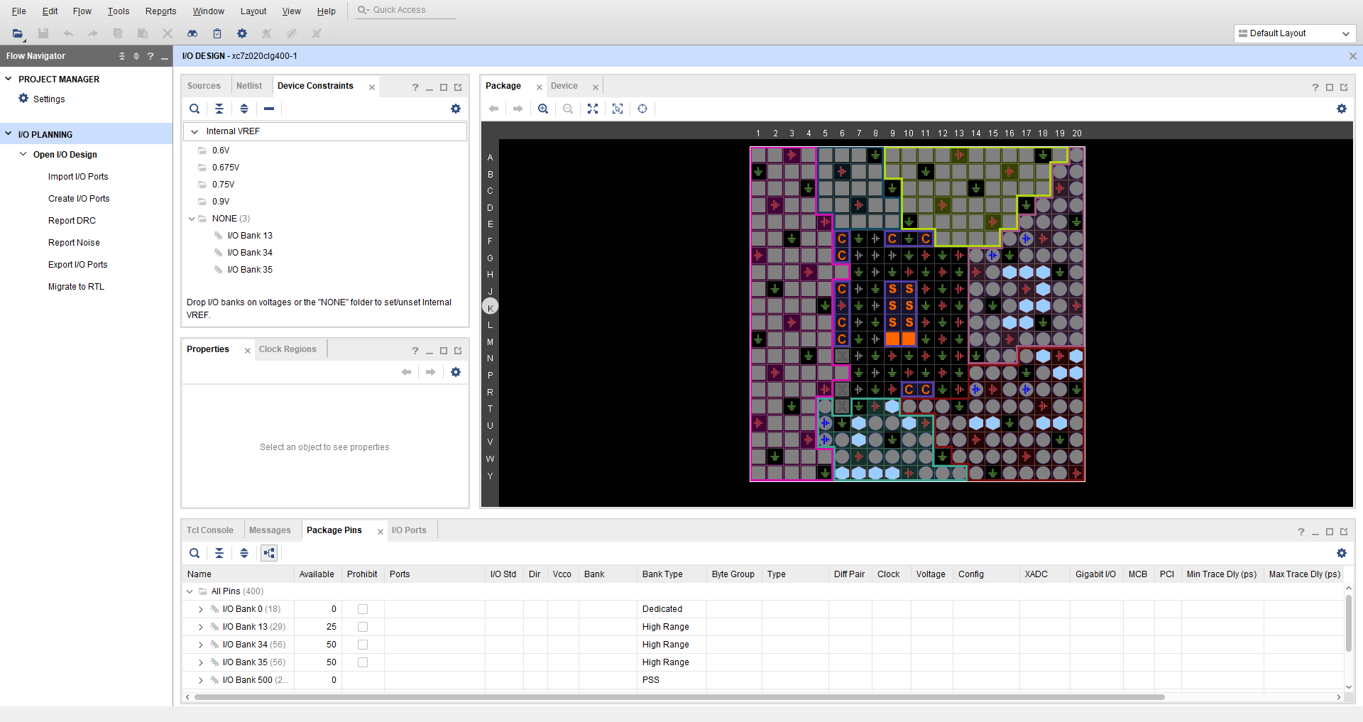
I/O Planning project’s default windows and views (PYNQ-Z2)

I/O Planning project’s default windows and views (Boolean)
Step 2 Create I/O Ports, Assign Various Pins and Add Source Files
Create input ports for clk_pin, btn_pin and rst_pin.
-
Select Flow Navigator > I/O PLANNING > Open I/O Design > Create > Create I/O Ports.
The Create I/O Ports form will be displayed.
-
Type clk_pin in the Name field, select Input for the Direction and select LVCMOS33 as the I/O Standard, and click OK.
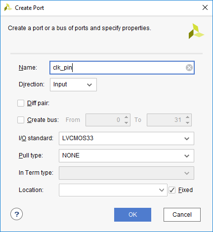
Creating I/O Port for clk_pin input
-
Similarly, create the btn_pin, rxd_pin and rst_pin input ports.
For PYNQ-Z2: Assign input pins clk_pin, btn_pin and rst_pin to H16, D19 and D20 locations using the Device view and package pins.
For Boolean: Assign input pins clk_pin, rxd_pin, btn_pin and rst_pin to F14, V12, J2 and J5 locations using the Device view and package pins.
(The images below take PYNQ-Z2 as example)
Hover the mouse over H16(PYNQ-Z2) or F14(Boolean) in the Device view window.
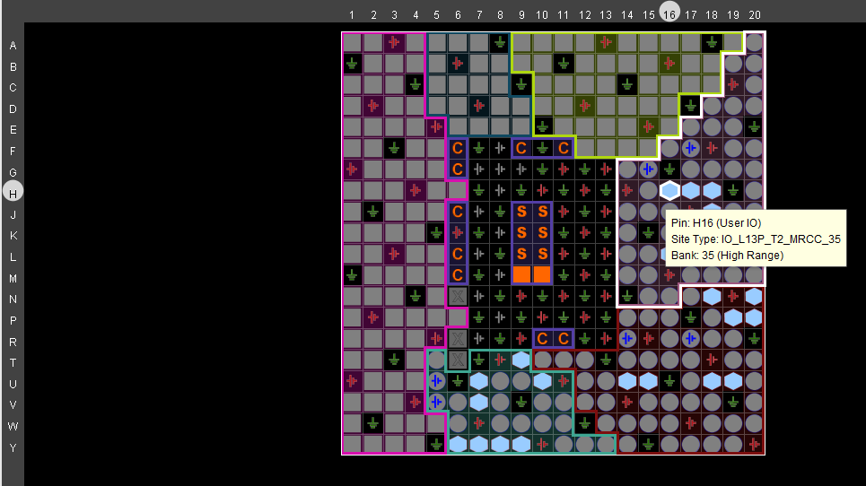
Locating H16 pin in the Device view(PYNQ-Z2)
-
When located, click on it.
The pin entry will be highlighted and displayed in the Package Pins tab.
-
In the Package Pins pane, click in the Ports column of H16(PYNQ-Z2) or F14(Boolean) pin’s row, and select clk_pin.
-
Similarly, add the btn_pin input port at D19(PYNQ-Z2) or J2(Boolean).
-
Select Edit > Find or Ctrl-F to open the Find form. Select Package Pins in the Find drop-down field, type D20(PYNQ-Z2) or J5(Boolean) in the match criteria field, and click on OK.

Finding a package pin(PYNQ-Z2)
Notice that the Find Results tab is opened, and the corresponding entry is shown in the tab.
-
Assign the rst_pin input to the pin J5(Boolean) or D20(PYNQ-Z2).
For PYNQ-Z2: Assign output pins led_pins[0] to led_pins[7] to locations B20, W8, U8, W6, Y7, F20, N16, M14. Create them as a vector and assign them using the Tcl command set_property. They all will be LVCMOS33.
For Boolean: Assign output pins led_pins[0] to led_pins[7] to locations R14, P14, N16, M14, W14, Y14, T11, T10. Create them as a vector and assign them using the Tcl command set_property. They all will be LVCMOS33.
Note: Notice that PYNQ has four LEDs hence we assign led_pins[3:0] to LEDs and led_pins[7:4] are assigned to PMODB.
-
In the I/O Ports tab, click on the create I/O port button on the left vertical ribbon.
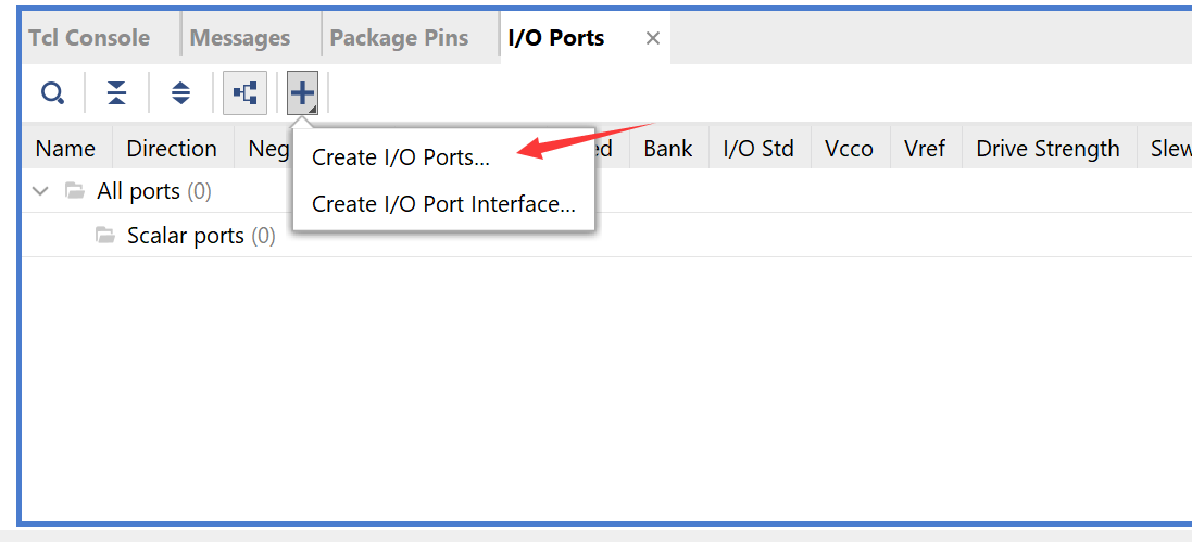
Create I/O Ports button
The Create I/O Ports form will be displayed.
-
Type led_pins in the Name field, select Output direction, click on the check-box of Create bus, set the msb to 7, and select LVCMOS33 I/O standard and click OK.
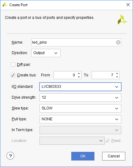
Creating I/O ports for the led_pins output
The led_pins entries will be created and displayed in the I/O Ports tab. Notice that the I/O standard and directions are already set, leaving only the pin locations to be assigned.
-
Type the following commands in the console to assign the pin locations.
For PYNQ-Z2:
# four on-board LEDs
set_property -dict { PACKAGE_PIN R14 IOSTANDARD LVCMOS33 } [get_ports { led_pins[0] }];
set_property -dict { PACKAGE_PIN P14 IOSTANDARD LVCMOS33 } [get_ports { led_pins[1] }];
set_property -dict { PACKAGE_PIN N16 IOSTANDARD LVCMOS33 } [get_ports { led_pins[2] }];
set_property -dict { PACKAGE_PIN M14 IOSTANDARD LVCMOS33 } [get_ports { led_pins[3] }];
# four LEDs on the RPi extension board
set_property -dict { PACKAGE_PIN B20 IOSTANDARD LVCMOS33 } [get_ports { led_pins[4] }];
set_property -dict { PACKAGE_PIN W8 IOSTANDARD LVCMOS33 } [get_ports { led_pins[5] }];
set_property -dict { PACKAGE_PIN U8 IOSTANDARD LVCMOS33 } [get_ports { led_pins[6] }];
set_property -dict { PACKAGE_PIN W6 IOSTANDARD LVCMOS33 } [get_ports { led_pins[7] }];
For Boolean:
set_property -dict {PACKAGE_PIN G1 IOSTANDARD LVCMOS33} [get_ports {led_pins[0]}] set_property -dict {PACKAGE_PIN G2 IOSTANDARD LVCMOS33} [get_ports {led_pins[1]}] set_property -dict {PACKAGE_PIN F1 IOSTANDARD LVCMOS33} [get_ports {led_pins[2]}] set_property -dict {PACKAGE_PIN F2 IOSTANDARD LVCMOS33} [get_ports {led_pins[3]}] set_property -dict {PACKAGE_PIN E1 IOSTANDARD LVCMOS33} [get_ports {led_pins[4]}] set_property -dict {PACKAGE_PIN E2 IOSTANDARD LVCMOS33} [get_ports {led_pins[5]}] set_property -dict {PACKAGE_PIN E3 IOSTANDARD LVCMOS33} [get_ports {led_pins[6]}] set_property -dict {PACKAGE_PIN E5 IOSTANDARD LVCMOS33} [get_ports {led_pins[7]}] -
Select File > Constraints > Save.
The Save Constraints form will be displayed.
-
Enter uart_led_{BOARDS} in the File name field, and click OK.

Saving constraints
The uart_led_{BOARDS}.xdc file will be created and added to the Sources tab.
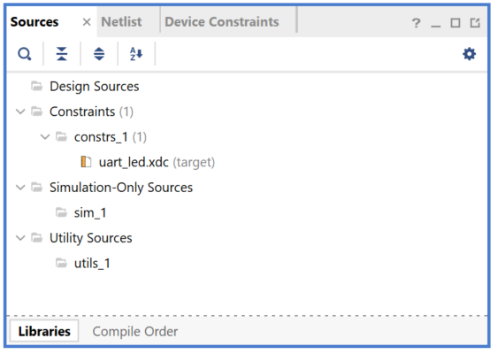
The uart_led.xdc file added to the source tree
-
Expand the Flow Navigator > I/O PLANNING > Open I/O Design > Report DRC.
-
Click OK. Notice the design rules checker has run and warnings are reported. Ignore the warnings.
-
Expand the Flow Navigator > I/O PLANNING > Open I/O Design > Report Noise and click OK. Notice the noise analysis is done on the output pins only (led_pins) and the results are displayed.
-
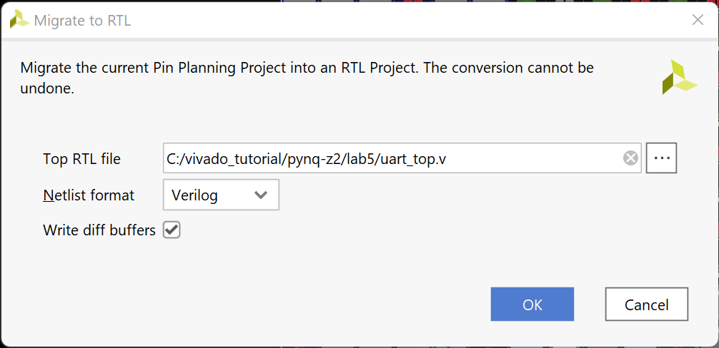
Click on Migrate to RTL.
The Migrate to RTL form will be displayed with Top RTL file field showing {TUTORIAL}/io_1.v entry.
-
Change io_1.v to uart_led.v(for PYNQ-Z2) or uart_top.v(for Boolean), and click OK
Assigning top-level file name(for Boolean)
-
Select the Hierarchy tab and notice that the uart_top.v file has been added to the project with top-level module name as ios. If you double-click the entry, you will see the module name with the ports listing.
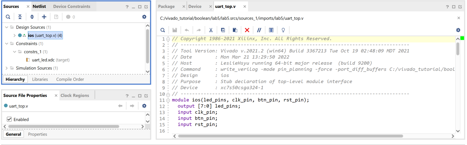
The top-level module content and the design hierarchy after migrating to RTL
Add the provided source files (from {SOURCES}/{BOARDS}/lab5) to the project. Copy the uart_led.txt (located in the {SOURCES}/{BOARDS}/lab5) content into the source file.
- Click Flow Navigator > Add Sources.
- In the Add Sources form, select Add or Create Design Sources, and click Next.
- Click on the Blue Plus button, then the Add Files…
- Browse to {SOURCES}\lab5 and select all .v(led_ctl.v, meta_harden.v, uart_baud_gen.v, uart_led.v, uart_rx.v uart_rx_ctl.v) files and click OK.
- Click Finish.
- Using Windows Explorer, browse to {SOURCES}\{BOARD}\lab5 and open uart_top.txt using any text editor. Copy the content of it and paste it in uart_top.v or uart_led.v in the Vivado project.
For PYNQ-Z2, there are two extra steps to do
-
In the Tcl Shell window enter the following command to change to the lab directory and hit the Enter key.
cd {TUTORIAL}/lab5 -
Generate the PS design by executing the provided Tcl script.
source ps_init.tclThis script will create a block design called system, instantiate ZYNQ PS with one GPIO channel (GPIO14) and one EMIO channel. It will then create a top-level wrapper file called system_wrapper.v which will instantiate the system.bd (the block design). You can check the contents of the tcl files to confirm the commands that are being run.
NOTICE: Please make sure that your top-level module is system_wrapper which is generated by the tcl script. If the auto-execute script fails, please manually set the system_wrapper as top. Right click on the system_wrapper entry, and click set as Top.
- Double-click on the uart_top(Boolean) or uart_led(PYNQ-Z2) entry to view its content.
Notice in the Verilog code, the BAUD_RATE and CLOCK_RATE parameters are defined to be 115200 and 125 MHz(PYNQ-Z2) or 100 MHz (Boolean) respectively.
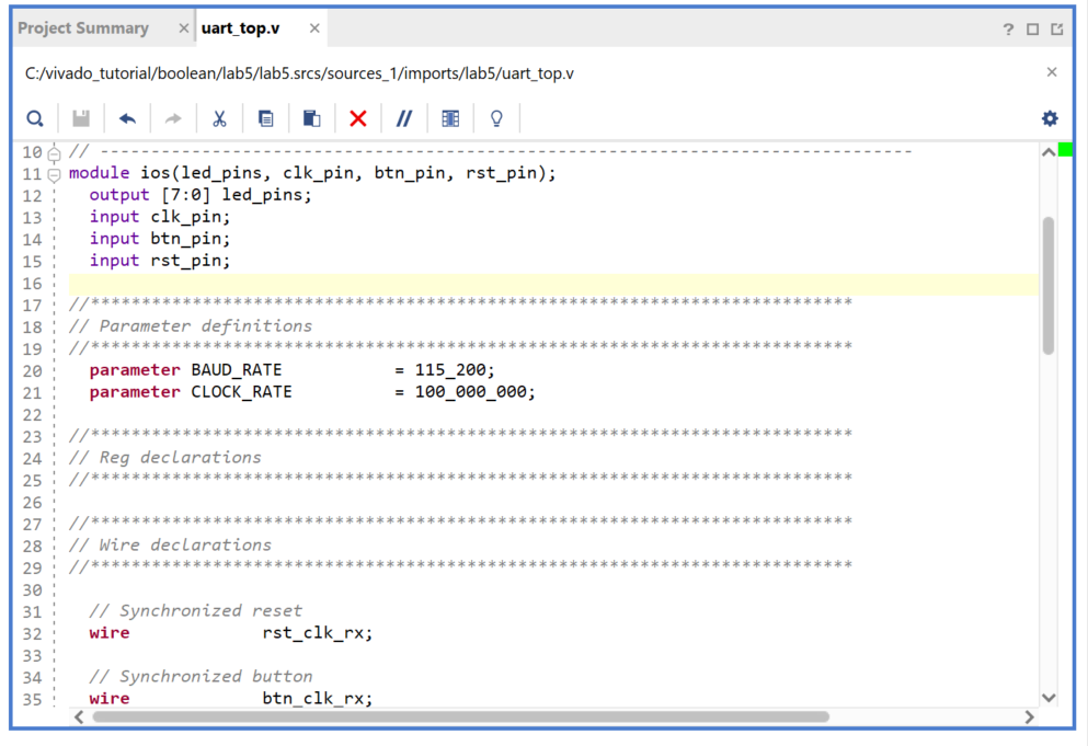
CLOCK_RATE parameter of uart_led
Step 3 Synthesize and Enter Timing Constraints
Synthesize the design. Use the Constraints Wizard to specify a clock frequency, and input and output delay constraints.
-
Click on the Run Synthesis in the Flow Navigator pane.
Click on the Save if save project window appears.
When synthesis is completed a form with three options will be displayed.
-
Select Open Synthesized Design and click OK.
-
In the Flow Navigator pane (under Open Synthesized Design), click on the Constraints Wizard. This will open up the Constraints Wizard.
-
Read the Identify and Recommend Missing Timing Constraints screen of the wizard to understand what the wizard does and click Next.
-
Specify the frequency of the object clk_pin to be 125 MHz(PYNQ-Z2) or 100MHz(Boolean), notice the Period, Rise At and Fall At are automatically populated. Also notice the Tcl command that can be previewed at the bottom of the wizard. Click Next to proceed.
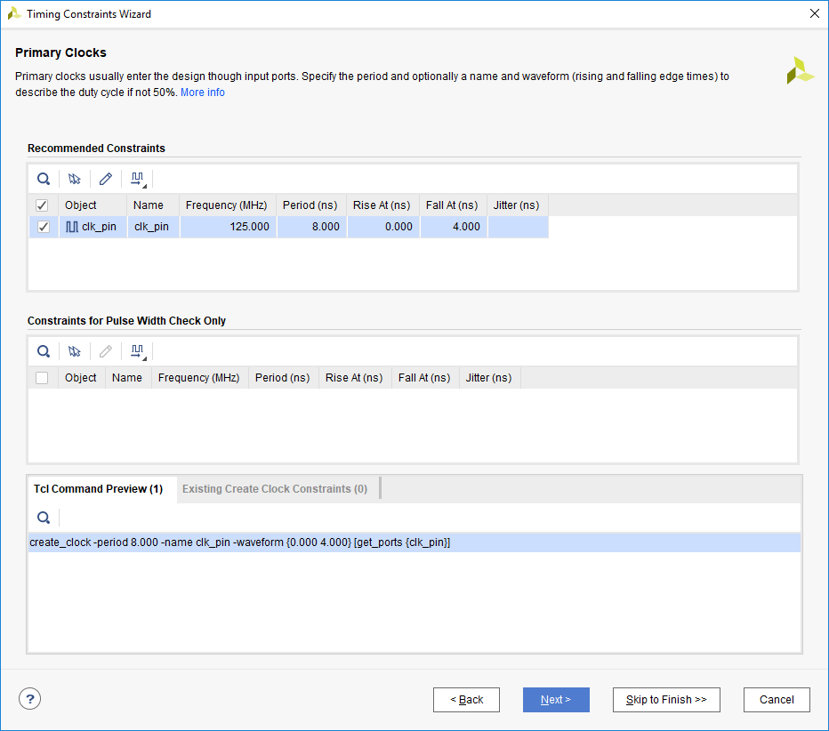
Constraints Wizard clk_pin parameters and Tcl command
-
There are no missing Generated Clocks, click Next to proceed.
-
There are no missing Forwarded Clocks, click Next to proceed.
-
There are no missing External Feedback Delays, click Next to proceed.
-
The wizard identifies Input Delays needed for the btn_pin, rxd_pin(Boolean ONLY) and rst_pin pins. Do the following:
- Press Ctrl and select the two rows.
- Enter the tco_min value to be -0.5 ns and everything else as 0 ns. Click Apply.
- Notice that under the Tcl Command Preview tab, 4 Tcl commands have been generated.
- Click Next.
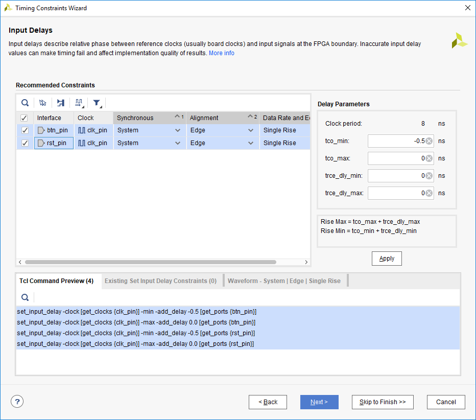
Specifying Input Delays for btn_pin and rst_pin(PYNQ-Z2)
-
Enter the tsu and thd as 0 ns and enter the trce_dly_max and trce_dly_min as -2.20 ns. Click Apply and then click Next.
-
There are no Combinatorial Delays identified, click Next to proceed.
-
Click Skip to Finish to skip to the final Constraints Summary page. Read the description of each page.
-
Check On Finish – View Timing Constraints and click Finish to close the wizard. The option will open the Timing Constraints Editor to show you the generated timing constraint.
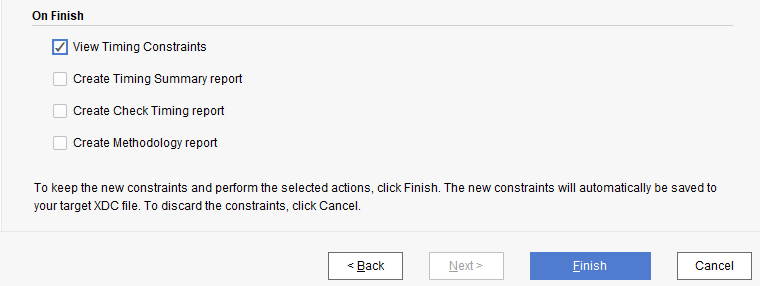
Selecting View Timing constraints
-
Note the wizard generated the clk_pin constraint for a 8 ns period (or 125 MHz)(PYNQ-Z2) or 10 ns period (or 100MHz)(Boolean). Notice in the All Constraints window, 7/9 constraints will be created.
There is no need to click Apply since the constraints have already been applied in the Constraints Wizard.
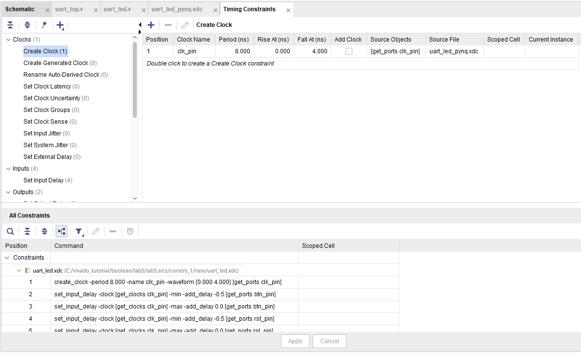
<p align = "center">
<i>The constraints added after using the Constraints Wizard</i>
</p>
- Open **uart_led_
.xdc** (if it was already opened, click **Reload** in the yellow status bar) and notice additional constraints were added to the last line of the file.
Generate an estimated Timing Report showing both the setup and hold paths in the design.
-
Select Flow Navigator > SYNTHESIS > Open Synthesized Design > Report Timing Summary.
-
In the Options tab, select min_max from the Path delay type drop-down list.
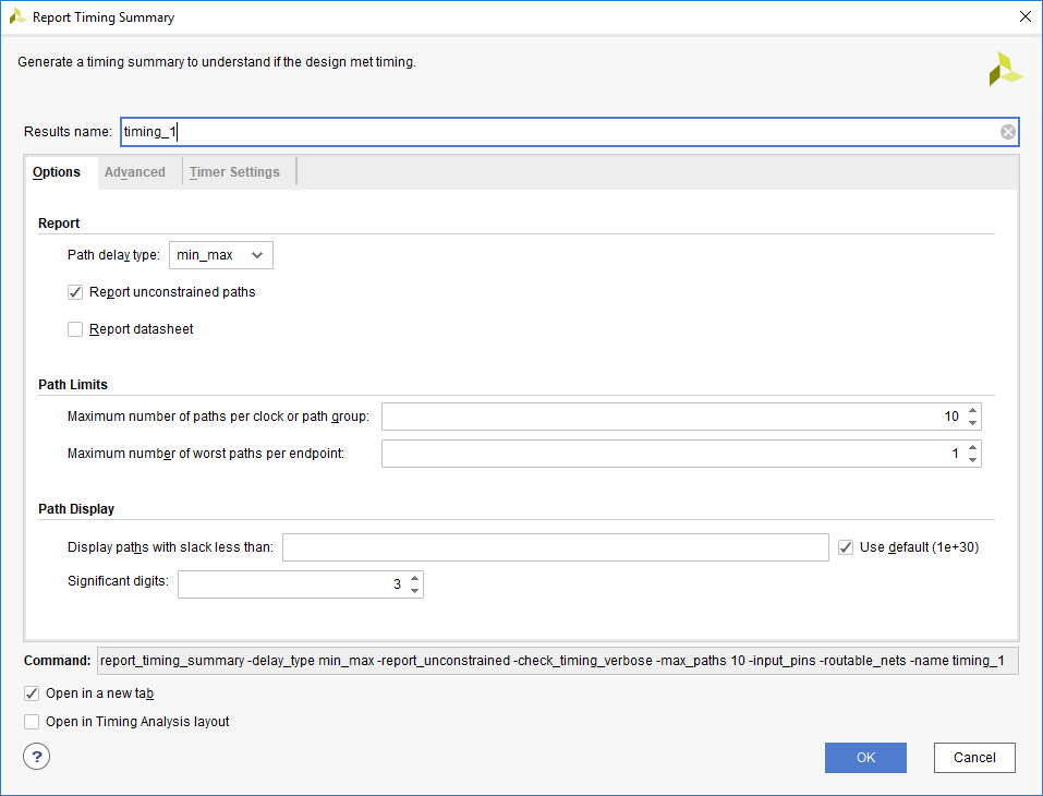
Performing timing analysis
-
Click OK to run the analysis.
The Timing Results view opens at the bottom of the Vivado IDE.
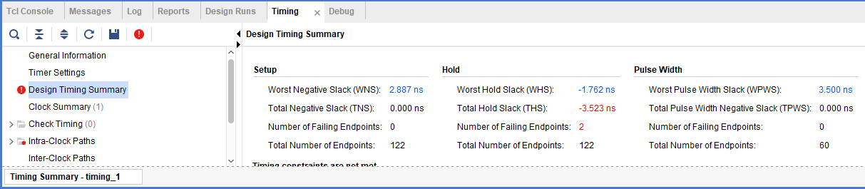
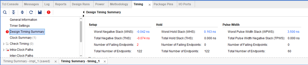
Timing summary
The Design Timing Summary report provides a brief worst Setup and Hold slack information and Number of failing endpoints to indicate whether the design has met timing or not.
Note that there are two timing failures under the hold check.
-
Click on the link next to Worst Hold Slack (WHS) to see the list of failing paths.
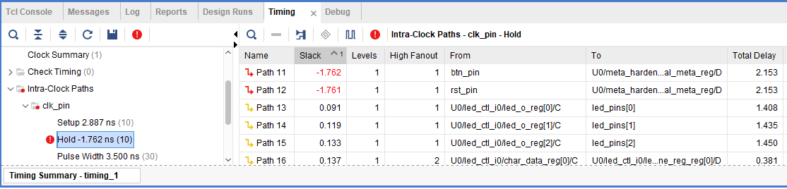
The list of paths showing hold violations
-
Double-click on the Path 11 to see the actual path detail.

Failing hold path
-
Select Path 11, right-click and select Schematic.

The schematic of the failing path
Step 4 Implement and Analyze Timing Summary
Implement the design.
-
Click on the Run Implementation.
-
Click Yes to run the synthesis first before running the implementation process.
When the implementation is completed, a dialog box will appear with three options.
-
Select the Open Implemented Design option and click OK.
-
Click Yes if you are prompted to close the synthesized design.
Generate a timing summary report
-
Select Flow Navigator > IMPLEMENTATION > Open Implemented Design > Report Timing Summary.
-
Click OK to generate the report using the default settings.
The Design Timing Summary window opens at the bottom in the Timing tab.
Note that failing timing paths are indicated in red.
Failing setup paths
-
Click on the WNS to see the failing paths.
-
Double-click on the first failing path from the top and see the detailed analysis.
The output path delay can be reduced by placing the register in IOB.
-
Apply the constraint by typing the following two commands in the Tcl console.
Hint: The implemented results are dependent on your own computer, if possible, tunning the output delay towards appropriate value to meet the timing constrains. As our testing shows, normally 0 ~ -4 ns will be a practical value.
set_output_delay -clock [get_clocks clk_pin] -min -add_delay -4 [get_ports {led_pins[*]}] set_output_delay -clock [get_clocks clk_pin] -max -add_delay -4 [get_ports {led_pins[*]}] -
Select File > Constraints > Save. Click OK at the warning message. Click Yes to save the project.
-
Click on Run Implementation.
-
Click Yes to reset the synthesis run, perform the synthesis, and run implementation.
-
Open the implemented design and observe that the number of failing paths in the Design Runs tab reported is 0.
-
Click Report Timing Summary, and observe that there are no failing paths.
Step 5 Generate the Bitstream and Verify the Functionality (Optional)
Generate the bitstream.
- Click Flow Navigator > PROGRAM AND DEBUG > Generate Bitstream.
- The write_bitstream command will be executed (you can verify it by looking in the Tcl console).
- Click Cancel when the bitstream generation is completed.
For Boolean:
Connect the board and power it ON. Open a hardware manager session, and program the FPGA.
- Make sure that the micro-USB cable is connected to the JTAG PROG connector (next to the power supply connector). Make sure that the jumper on the board is set to select USB power.
- Select the Open Hardware Manager option and click OK. The Hardware Manager window will open indicating “unconnected” status.
-
Click on the Open target link, then Auto Connect from the dropdown menu.

Opening new hardware target
- The Hardware Session status changes from Unconnected to the server name and the device is highlighted. Also notice that the Status indicates that it is not programmed.
- Select the device in the Hardware Device Properties, and verify that the uart_led.bit is selected as the programming file in the General tab.
For PYNQ-Z2:
Insert the SD card, Connect the board and power it ON. Open a hardware manager session, and program the FPGA.
- Copy the provided SD card boot image ({SOURCES}/lab5/BOOT.bin) into a blank SD card, noticing that file system of SD card should be FAT32.
- Insert the SD card to the SD card slot on the back of the board and set the booting jumper to SD.
-
Select the Open Hardware Manager option and click OK. The Hardware Manager window will open indicating “unconnected” status.
Opening new hardware target
- The Hardware Session status changes from Unconnected to the server name and the device is highlighted. The status may indicate that the device is programmed, ignore the status.
-
Select the device in the Hardware Device Properties, and verify that the system_wrapper.bit is selected as the programming file in the General tab.
-
Make sure that the Micro-USB cable is connected to the JTAG PROG connector.
-
Turn ON the power.
-
Select the Open Hardware Manager option.
The Hardware Manager window will open indicating “unconnected” status.
-
Click on the Open target link, then Auto Connect from the dropdown menu.
You can also click on the Open recent target link if the board was already targeted before.
-
The Hardware Manager status changes from Unconnected to the server name and the device is highlighted. Also notice that the Status indicates that it is not programmed.
- Select the device and verify that the ios.bit is selected as the programming file in the General tab.
Start a terminal emulator program such as TeraTerm or Mobaxterm. Select an appropriate COM port (you can find the correct COM number using the Control Panel). Set the COM port for 115200 baud rate communication. Program the FPGA and verify the functionality.
-
Start a terminal emulator program such as TeraTerm or Mobaxterm.
-
Select an appropriate COM port (you can find the correct COM number using the Control Panel).
-
Set the COM port for 115200 baud rate communication.
-
Right-click on the FPGA entry in the Hardware window and select Programming Device…
-
Click on the Program button.
The programming bit file be downloaded and the DONE light will be turned ON indicating the FPGA has been programmed.
-
Type in some characters in the terminal emulator window and see the corresponding ASCII equivalent bit pattern displayed on the LEDs.
-
Press and hold BTNU and see the the upper four bits are swapped with the lower four bits on the LEDs.
-
When satisfied, select File > Close Hardware Manager. Click OK.
-
close the terminal emulator program and power OFF the board.
-
Close the Vivado program by selecting File > Exit and click OK.
Conclusion
In this lab, you learned how to create an I/O Planning project and assign the pins via the Device view, Package Pins tab, and the Tcl commands. You then exported to the rtl project where you added the provided source files. Next you created timing constraints and performed post-synthesis and post-implementation timing analysis.
Copyright© 2023, Advanced Micro Devices, Inc.