Hardware Debugging
Introduction
In this lab you will use the uart_led design that was introduced in the previous labs. You will use Mark Debug feature and also the available Integrated Logic Analyzer (ILA) core (in IP Catalog) to debug the hardware.
Objectives
After completing this lab, you will be able to:
-
Use the Integrated Logic Analyzer (ILA) core from the IP Catalog as a debugging tool.
-
Use Mark Debug feature of Vivado to debug a design.
-
Use hardware debugger to debug a design.
Design Description
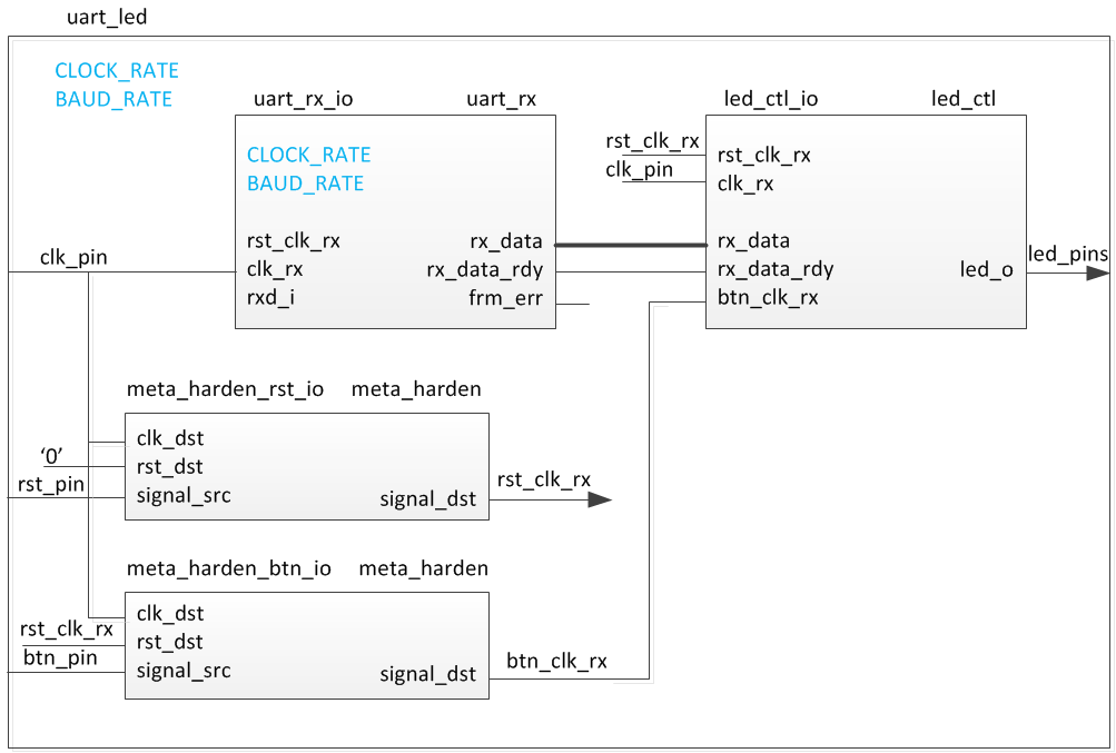
The design consists of a uart receiver receiving the input typed on a keyboard and displaying the binary equivalent of the typed character on the LEDs. When a push button is pressed, the lower and upper nibbles are swapped.
For PYNQ-Z2
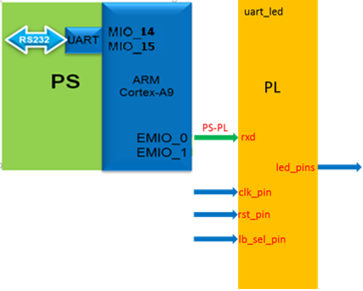
In this design we will use board’s USB-UART which is connected to, and controlled by the Zynq’s ARM Cortex-A9 processor. Our PL design needs access to this USB-UART. We will use a Processing System (PS) design which will make the USB-UART connection available to the PL.
The provided design places the UART (RX) pin of the PS on the Cortex-A9 in a simple GPIO mode to allow the UART to be connected (passed through) to the programmable logic. The PS samples the RX signal and sends it to the EMIO channel 0 which is connected to RX input of the HDL design. This is done through a software application provided in the lab6.sdk directory.
For Boolean:
The Boolean board is more straightforward. It has a UART port connected directly to the FPGA which will be used in this design.
The Complete Design on PYNQ-Z2's PL Side or Whole Design on Boolean
The Complete System on PYNQ-Z2
General Flow
flowchart TD
1:[Step1: Create a Vivado Project] --> 2:[Step2: Add the ILA Core] --> 3:[Step3: Synthesize the Design and Mark Debug] --> 4:[Step4: Implement and Generate Bitstream] -->5:[Step5: Debug in Hardware]
Instructions for the Tutorial
The absolute path for the source code should only contain ascii characters. Deep path should also be avoided since the maximum supporting length of path for Windows is 260 characters.
{BOARD} refers to target Boolean and Z2 boards.
{SOURCES} refers to ./source/{BOARD}/labn. You can use the source files from the cloned repository’s source directory
{TUTORIAL} refers to C:\vivado_tutorial/. It assumes that you will create the mentioned directory structure to carry out the labs of this tutorial
Steps
Step 1 Create a Vivado Project using IDE
For PYNQ-Z2:
Launch Vivado and create a project targeting the XC7Z020clg400-1 device, and use the provided tcl script file (ps_init.tcl) to generate the block design for the PS subsystem. Also, add the Verilog HDL files, uart_led_pins_pynq.xdc and uart_led_timing_pynq.xdc files from the {SOURCES}\lab5 directory.
For Boolean:
Launch Vivado and create a project targeting XC7S50CSGA324-1 parts, and using the Verilog HDL. Use the provided Verilog source files and XDC files from the {SOURCES}\lab6\ directory.
-
Open Vivado by selecting Start > Xilinx Design Tools > Vivado 2021.2.
-
Click Create New Project to start the wizard. You will see Create A New Vivado Project dialog box. Click Next.
-
Click the Browse button of the Project location field of the New Project form, browse to {TUTORIAL}, and click Select.
-
Enter lab6 in the Project name field. Make sure that the Create Project Subdirectory box is checked. Click Next.
-
Select RTL Project option in the Project Type form, and click Next.
-
Using the drop-down buttons, select Verilog as the Target Language and Simulator Language in the Add Sources form.
-
Click on the Blue Plus button, then the Add Files… button and browse to the {SOURCES}/{BOARD}/lab6 directory, select all the Verilog files (led_ctl.v, meta_harden.v, uart_baud_gen.v, uart_led.v, uart_rx.v and uart_rx_ctl.v ), click OK, and then click Next.
-
Click Next to get to the Add Constraints form.
-
Click on the Blue Plus button, then Add Files… and browse to the {SOURCES}/{BOARDS}\lab6 directory (if necessary), select uart_led_timing_{BOARDS}.xdc and the appropriate uart_led_pins_{BOARDS}.xdc and click Open.
-
Click Next.
-
In the Default Part form, use the Parts option and various drop-down fields of the Filter section, select the XC7Z020clg400-1(PYNQ-Z2) or XC7S50CSGA324-1(Boolean) part.
-
Click Next.
-
Click Finish to create the Vivado project.
If you are using PYNQ-Z2
-
Copy the
ps_init.tclto the path {TUTORIAL}/lab6. In the Tcl Shell window enter the following command to change to the lab directory and hit the Enter key.cd {TUTORIAL}/lab6 -
Generate the PS design by executing the provided Tcl script.
source ps_init.tclThis script will create a block design called system, instantiate ZYNQ PS with one GPIO channel (GPIO14) and one EMIO channel. It will then create a top-level wrapper file called system_wrapper.v which will instantiate the system.bd (the block design). You can check the contents of the tcl files to confirm the commands that are being run.
-
Double-click on the uart_led entry to view its content.
Notice in the Verilog code, the BAUD_RATE and CLOCK_RATE parameters are defined to be 115200 and 125 MHz(PYNQ-Z2) and 100 MHz(Boolean) respectively.

CLOCK_RATE parameter of uart_led(PYNQ-Z2 as Example)
Step 2 Add the ILA Core
-
Click Flow Navigator > PROJECT MANAGER > IP Catalog.
The catalog will be displayed in the Auxiliary pane.
-
Expand the Debug & Verification > Debug folders and double-click the ILA(Integrated Logic Analyzer) entry.
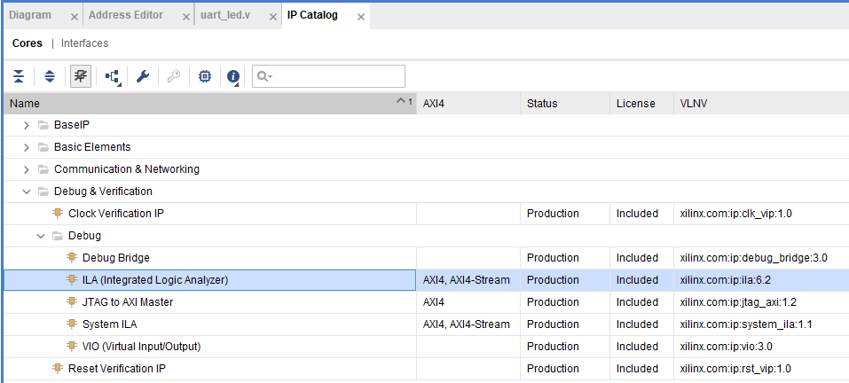
ILA in IP Catalog
You will be connecting the ILA core/component to the LED port which is 8-bit wide.
-
Double click the ILA(Integrated Logic Analyzer > Customize IP on the following Add IP window. The ILA IP will open.
-
Change the component name to ila_led.
-
Change the Number of Probes to 2.
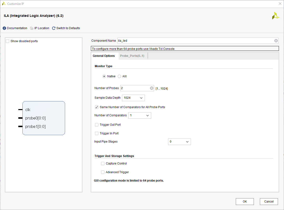
Setting the component name and the number of probes field
-
Select the Probe Ports tab and change the PROBE1 port width to 8, leaving the PROBE0 width to 1.
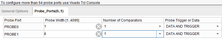
Setting the probes widths
-
Click OK.
The Generate Output Products dialog box will appear.
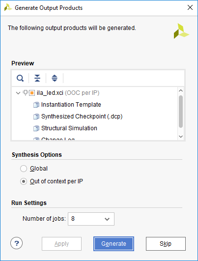
The Generate Output Products
-
Click the Generate button to generate the core including the instantiation template. Click OK at the warning box. Notice the core is added to the Design Sources view.

Newly generated ILA core added in the design source(PYNQ-Z2)
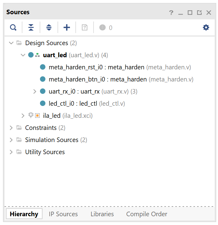
Newly generated ILA core added in the design source(Boolean)
-
Select the IP Sources tab, expand the IP(1) > ila_led > Instantiation Template, and double-click the ila_led.veo entry to see the instantiation template.
-
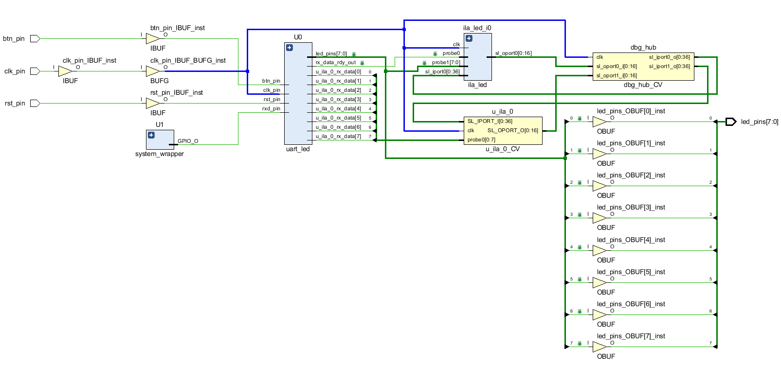
Instantiate the ila_led in design by copying lines 56 – 62 and pasting to ~line 69(PYNQ-Z2) or 107(Boolean) (before “endmodule” on the last line) in the top module.
-
Change your_instance_name to ila_led_i0.
-
Change the following port names in the Verilog code to connect the ila to existing signals in the design:
.clk(CLK)          . clk(clk_pin)

.probe0(PROBE0)   . probe0(rx_data_rdy)

.probe1(PROBE1)   . probe1(led_pins)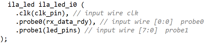
Instantiating the ILA Core in the uart_top.v
-
Select File > Save File.
Notice that the ILA Core instance is in the design hierarchy.

ILA Core added to the design(PYNQ-Z2)
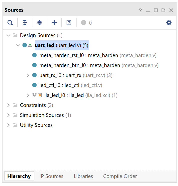
ILA Core added to the design(Boolean)
Step 3 Synthesize the Design and Mark Debug
Synthesize the design. Open the synthesized design. View the schematic. Add Mark Debug on the rx_data bus between the uart_rx_i0 and led_ctl_i0 instances.
-
Click Flow Navigator > SYNTHESIS > Run Synthesis. Click Save to save Project if prompted.
The synthesis process will be run on the uart_top.v and all its hierarchical files. When the process is completed a Synthesis Completed dialog box with three options will be displayed.
-
Select the Open Synthesized Design option and click OK.
-
Click on Flow Navigator > SYNTHESIS > Synthesized Design > Schematic to view the synthesized design in a schematic view.
-
Expand component U0(PYNQ-Z2) or uart_rx_i0(Boolean) and Select the rx_data bus between the uart_rx_i0 and the led_ctl_i0 instances or right-click, and select Mark Debug.

Marking a bus to debug(PYNQ-Z2)
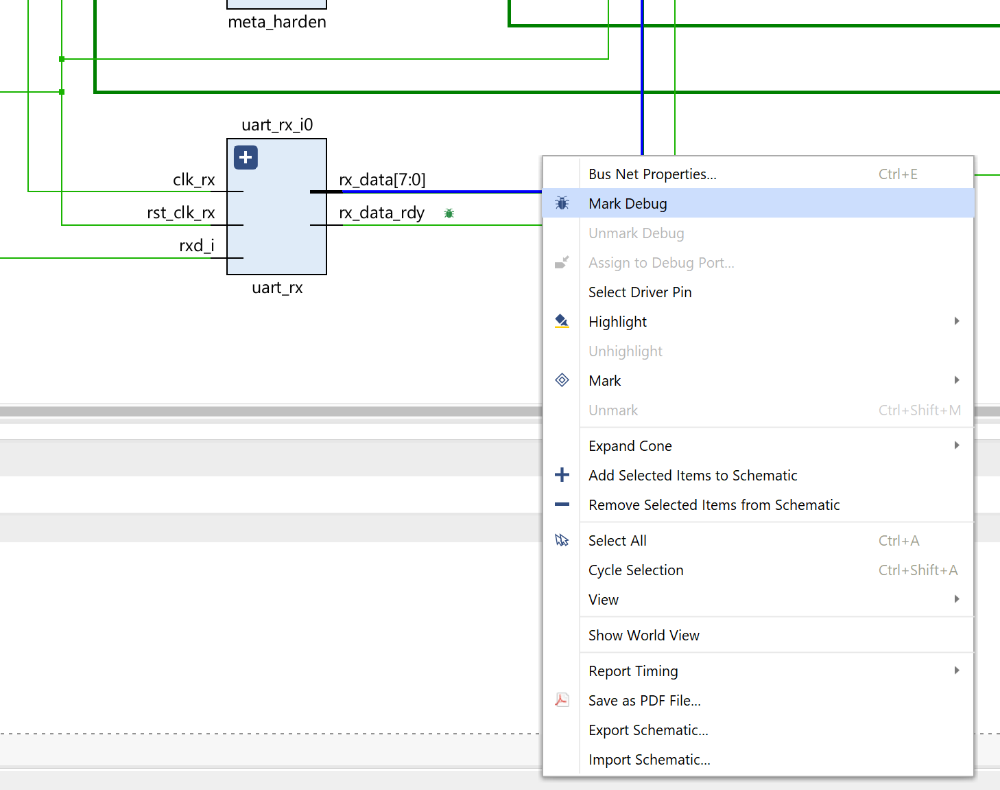
Marking a bus to debug(Boolean)
-
Select File > Constraints > Save.
-
Click OK, and then again OK to use uart_led_timing_{BOARDS}.xdc as the target.
-
Select the Netlist tab and notice that the nets which are marked/assigned for debugging have a debug icon next to them.
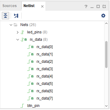
Nets with debug icons
-
Select the Debug layout or Layout > Debug.
Notice that the Debug tab is visible in the Console pane showing Assigned and Unassigned Debug Nets groups.

Debug tab showing assigned and unassigned nets
-
Either click on the
 button in the top vertical tool buttons of the Debug pane, or right-click on the Unassigned Debug Nets and select the Set up Debug… option.
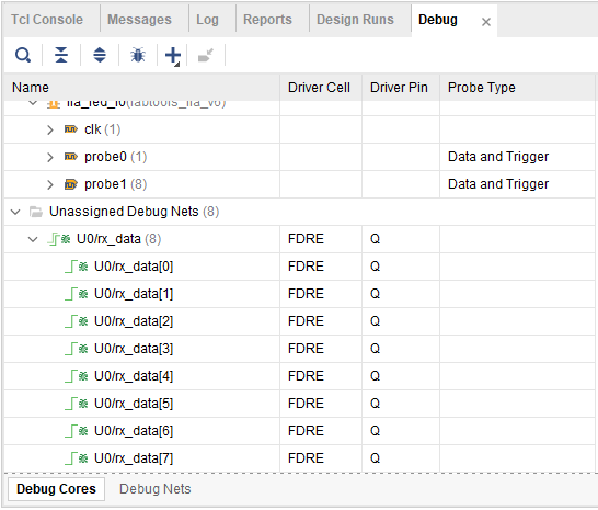
-
In the Set Up Debug wizard click Next.
Note that rx_data is listed, with the Clock Domain as clk_pin_IBUF_BUFG.
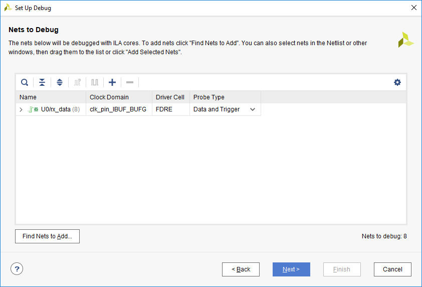
The remaining nets after removing already assigned nets in the Set Up Debug wizard
-
Click Next and again Next (leaving everything as defaults) then Finish.
-
In the Synthesized Design Schematic, click on the net on the output side of the BUFG for the input pin named clk_pin. Hover over the now highlighted net and notice the name is clk_pin_IBUF_BUFG. This is the clock net selected for the debug nets earlier.
Locating clk_pin_IBUF_BUFG in the design(PYNQ-Z2)

Locating clk_pin_IBUF_BUFG in the design(Boolean)
-
Right click on uart_led_pins_{BOARD}.xdc in the sources pane and select Set as Target Constraint File. This will save the changes to the file.
-
Select File > Constraints > Save and click OK and Click Yes.
-
Open uart_led_pins_{BOARDS}.xdc and notice the debug nets have been appended to the bottom of the file.
Step 4 Implement and Generate Bitstream
Generate the bitstream.
-
Click on the Generate Bitstream to run the implementation and bit generation processes.
-
Click Yes to run the implementation processes.
-
When the bitstream generation process has completed successfully, a box with three options will appear. Select the Open Hardware Manager option and click OK.
Step 5 Debug in Hardware
Connect the board and power it ON. Open a hardware manager session, and program the FPGA.
-
Make sure that the Micro-USB cable is connected to the JTAG PROG connector.
-
Turn ON the power.
-
Select the Open Hardware Manager option and click OK.
The Hardware Manager window will open indicating “unconnected” status.
-
Click on the Open target link, then Auto Connect from the dropdown menu.
You can also click on the Open recent target link if the board was already targeted before.
-
The Hardware Session status changes from Unconnected to the server name and the device is highlighted. Also notice that the Status indicates that it is not programmed.
-
Select the device and verify that the uart_top.bit is selected as the programming file in the General tab. Also notice that there is an entry in the Debug probes file field.
Start a terminal emulator program such as TeraTerm or HyperTerminal. Select an appropriate COM port (you can find the correct COM number using the Control Panel). Set the COM port for 115200 baud rate communication. Program the FPGA and verify the functionality.
-
Start a terminal emulator program such as TeraTerm or HyperTerminal.
-
Select an appropriate COM port (you can find the correct COM number using the Control Panel).
-
Set the COM port for 115200 baud rate communication.
-
Right-click on the FPGA, and select Program Device… and click Program. For PYNQ-Z2, the localhost will show “programmed”, ignore the status and program the device with generated bitstream.
The programming bit file be downloaded and the DONE light will be turned ON indicating the FPGA has been programmed. Debug Probes window will also be opened, if not, then select Window > Debug Probes.
In the Hardware window in Vivado notice that there are two debug cores, hw_ila_1 and hw_ila_2.
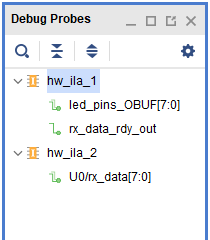
Debug probes
The hardware session status window also opens showing that the FPGA is programmed having two ILA cores with the idle state.
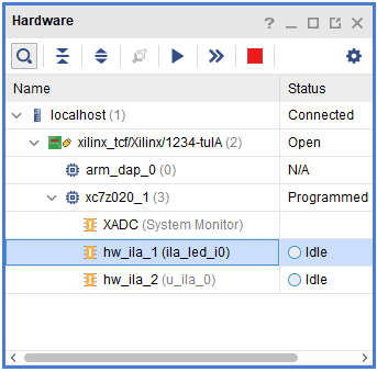
Hardware session status
Select the target FPGA xc7z020_1 or xc7s50_0, and click on the Run Trigger Immediate button to see the signals in the waveform window.

Opening the waveform window
Two waveform windows will be created, one for each ILA; one ILA window is for the instantiated ILA core and another for the MARK DEBUG method.
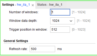
Setup trigger conditions to trigger on a write to led port (rx_data_rdy_out=1) and the trigger position to 512. Arm the trigger.
-
In the Trigger Setup window, click Add Probes and select the rx_data_rdy_out.
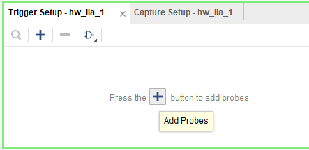
Adding a signal to trigger setup
-
Set the compare value (== [B] X) and change the value from x to 1. Click OK.
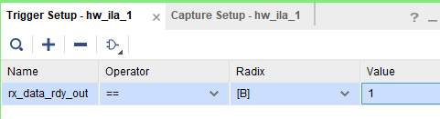
Setting the trigger condition
-
Set the trigger position of the hw_ila_1 to 512.
Setting up the trigger position
-
Similarly, set the trigger position of the hw_ila_2 to 512.
-
Select the hw_ila_1 in the Hardware window and then click on the Run Trigger (
 ) button. Observe that the hw_ila_1 core is armed and showing the status as Waiting for Trigger.
Hardware analyzer running in capture mode
-
In the terminal emulator window, type a character, and observe that the hw_ila_1 status changes from capturing to idle as the rx_data_rdy_out became 1.
-
Select the hw_ila_data_1.wcfg window and see the waveform. Notice that the rx_data_rdy_out goes from 0 to 1 at 512th sample.
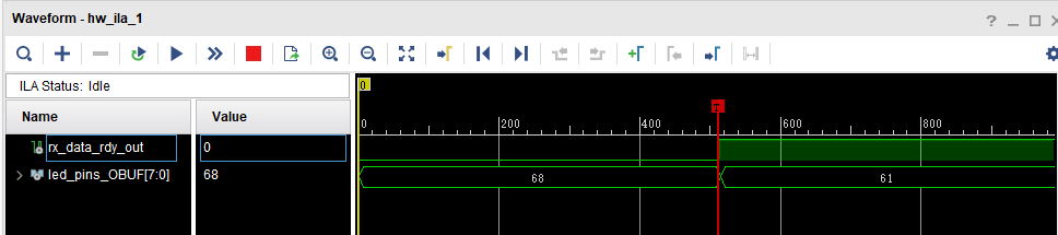
Zoomed waveform view
-
Add the hw_ila_2 probes to the trigger window of the hw_ila_2 and change the trigger condtion for rx_data[7:0]’s Radix from Hexadecimal to Binary. Change XXXX_XXXX to 0101_0101 (for the ASCII equivalent of U).

Setting up trigger condition for a particular input pattern
-
In the Hardware window, right-click on the hw_ila_2 and select Run Trigger, and notice that the status of the hw_ila_2 changes from idle to Waiting for Trigger. Also notice that the hw_ila_1 status does not change from idle as it is not armed.
-
Switch to the terminal emulator window and U (capital ,shift+u) to trigger the core.
-
Select the corresponding waveform window and verify that it shows 55 after the trigger.
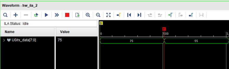
Second ila core triggered
-
When satisfied, Select File > Close Hardware Manager. Click OK to close it.
-
Close the terminal emulator program and power OFF the board.
-
Close the Vivado program by selecting File > Exit and click OK.
Conclusion
You used ILA core from the IP Catalog and Mark Debug feature of Vivado to debug the hardware design.
Copyright© 2023, Advanced Micro Devices, Inc.