Vitis HLS Design Flow Lab
Introduction
This lab provides a basic introduction to high-level synthesis using the Vitis HLS tool flow. You will use Vitis HLS in GUI mode to create a project. You will simulate, synthesize, and implement the provided design.
Objectives
After completing this lab, you will be able to:
- Create a new project using Vitis HLS in GUI mode
- Simulate a C design by using a self-checking test bench
- Synthesize the design
- Perform design analysis using the Analysis Perspective view
- Perform co-simulation on a generated RTL design by using a provided C test bench
- Implement a design
Steps
Create a New Project
Create a new project in Vitis HLS targeting PYNQ-Z2 board
-
Launch Vitis HLS: Select Start > Xilinx Design Tools > Vivado 2021.2 > Vitis HLS 2021.2
You can also invoke Vitis HLS from Vitis HLS Command prompt by selecting Start > Xilinx Design Tools > Vitis HLS 2021.2 Command Prompt and then typing vitis_hls in the terminal.
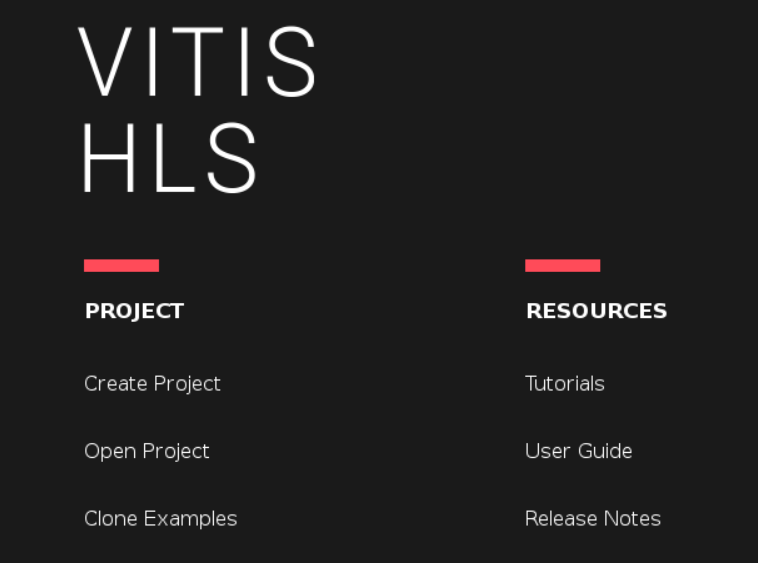
Getting Started view of Vitis HLS
- In the Getting Started GUI, click on Create Project. The New Vitis HLS Project wizard opens.
-
Click the Browse… button of the Location field and browse to {labs}\lab1 on a Windows machine or {labs}/lab1 on a Linux machine creating sub-folders as necessary, and then click OK.
Note: From this point onward reference will be made to Linux name.
- For Project Name, type matrixmul.
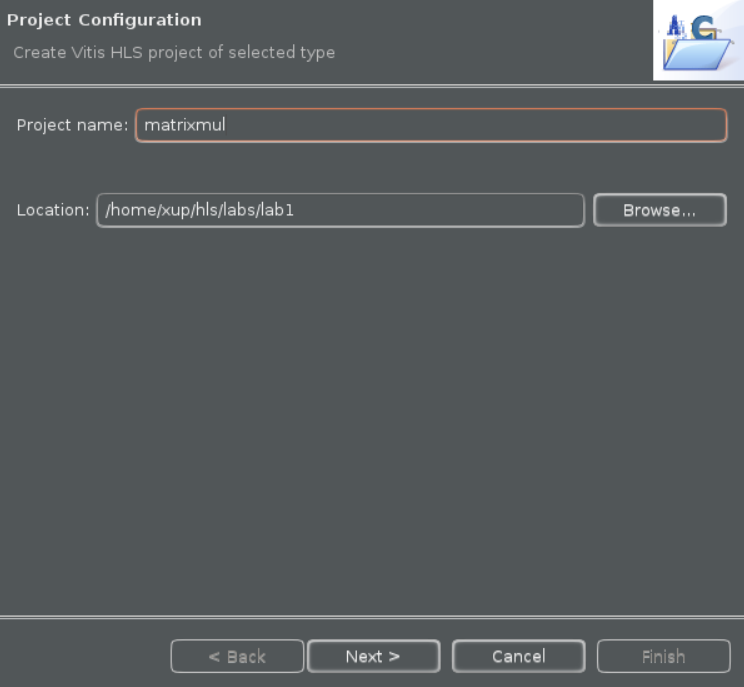
New Vitis HLS Project wizard
- Click Next.
- In the Add/Remove Design Files window, type matrixmul as the Top Function name (the provided source file contains the function, called matrixmul, to be synthesized).
- Click the Add Files… button, select matrixmul.cpp file from the {labs}/lab1 folder, and then click Open.
- Click Next.
- In the Add/Remove Testbench Files for the testbench, click the Add Files… button, select matrixmul_test.cpp file from the /home/xup/hls/labs/lab1 folder and click Open.
- Select the matrixmul_test.cpp in the files list window and click the Edit CFLAG… button, type -DHW_COSIM, and click OK. (This defines a compiler flag that will be used later.)
- Click Next.
- In the Solution Configuration page, leave Solution Name field as solution1 and set the clock period as 10.
- Click the … (browse) button of the Part Selection section.
- In the Device Selection page, select Parts Specify field, enter xc7z020clg400-1 in the Search field and click OK.
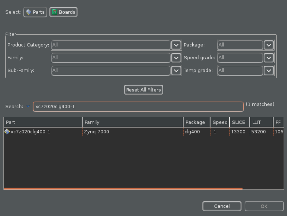
Using Parts Specify option in Part Selection Dialog
- Click Finish.
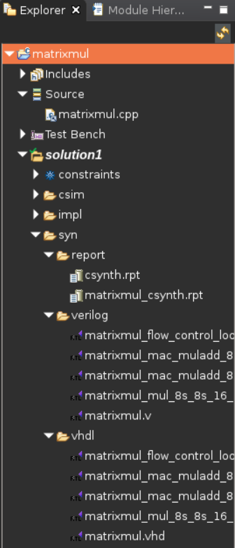
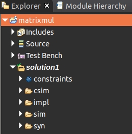
You will see the created project in the Explorer view. Expand various sub-folders to see the entries under each sub-folder.
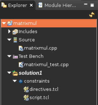
Explorer Window
- Double-click on the matrixmul.cpp under the source folder to open its content in the information pane.
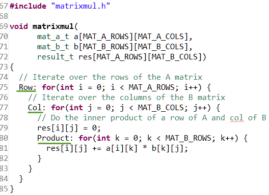
The Design under consideration
It can be seen that the design is a matrix multiplication implementation, consisting of three nested loops. The Product loop is the inner most loop performing the actual Matrix elements product and sum. The Col loop is the outer-loop which feeds the next column element data with the passed row element data to the Product loop. Finally, Row is the outer-most loop. The res[i][j]=0 (line 41) resets the result every time a new row element is passed and new column element is used.
Run C Simulation
- Select Project > Run C Simulation, and click OK in the C Simulation Dialog window.
The files will be compiled and you will see the output in the Console window.
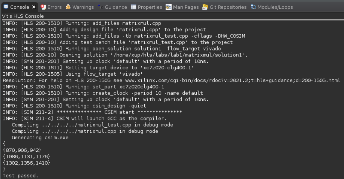
Program output
-
Double-click on matrixmul_test.cpp under testbench folder in the Explorer to see the content.
You should see two input matrices initialized with some values and then the code that executes the algorithm. If HW_COSIM is defined (as was done during the project set-up) then the matrixmul function is called and compares the output of the computed result with the one returned from the called function, and prints Test passed if the results match. If HW_COSIM had not been defined then it will simply output the computed result and not call the matrixmul function.
Run Debugger
Run the application in debugger mode and understand the behavior of the program.
-
Select Project > Run C Simulation. Select the Launch Debugger option and click OK.
The application will be compiled with –g option to include the debugging information, the compiled application will be invoked, and the debug perspective will be opened automatically.
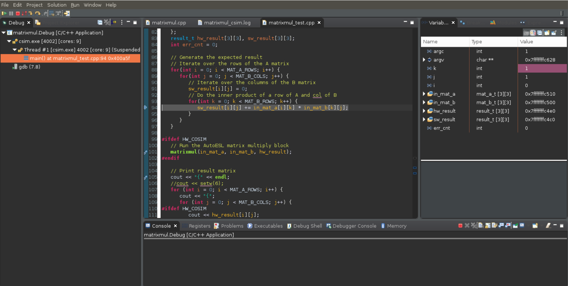
- The Debug perspective will show the matrixmul_test.cpp in the source view, argc and argv variables defined in the Variables view, thread created and the program suspended at the main() function entry point in the Debug view.
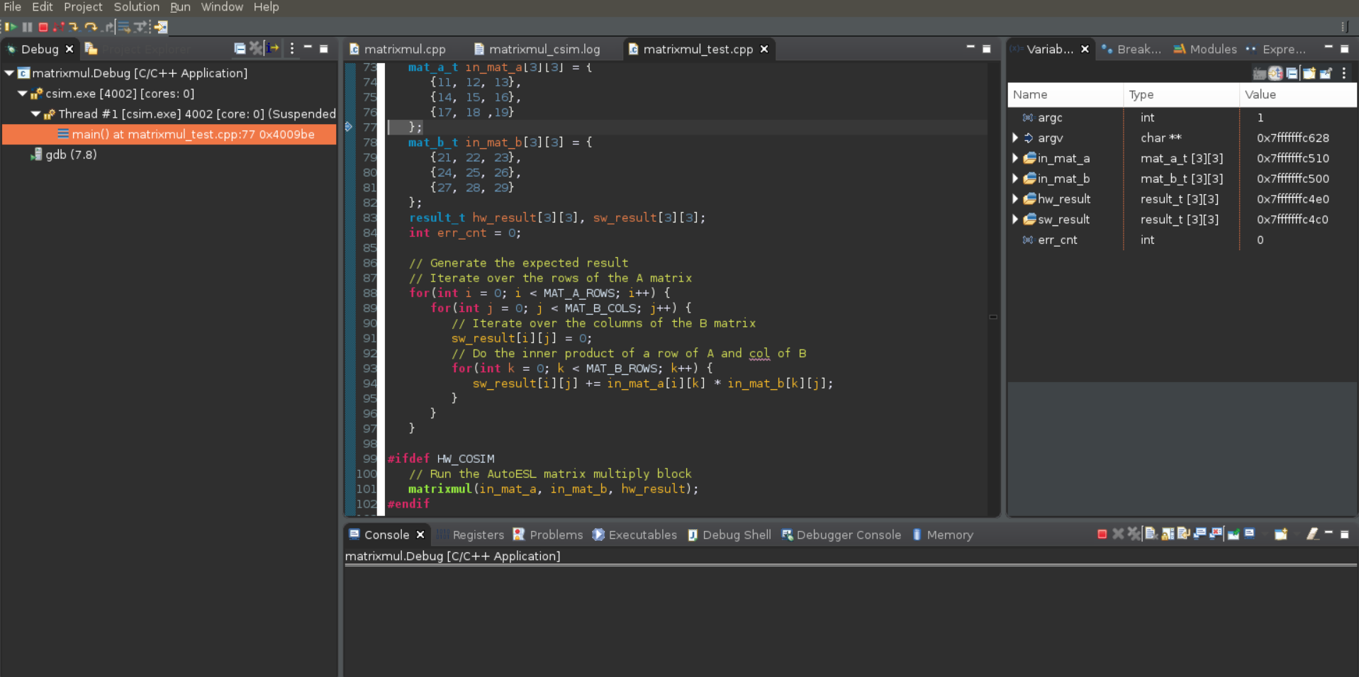
A Debug perspective
-
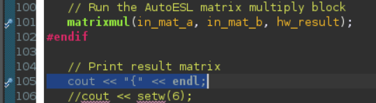
Scroll-down in the source view, and double-click in the blue margin at line 67 where it is about to output “{“ in the output console window. This will set a break-point at line 67.
The breakpoint is marked with a blue circle, and a tick.
- Similarly, set a breakpoint at line 63 in the matrixmul() function.
- Using the Step Over (F6) button several times, observe the execution progress, and observe the variable values updating, as well as computed software result.
Debugger’s intermediate output view
- Now click the Resume button or F8 to complete the software computation and stop at line 63.
- Observe the following computed software result in the variables view.
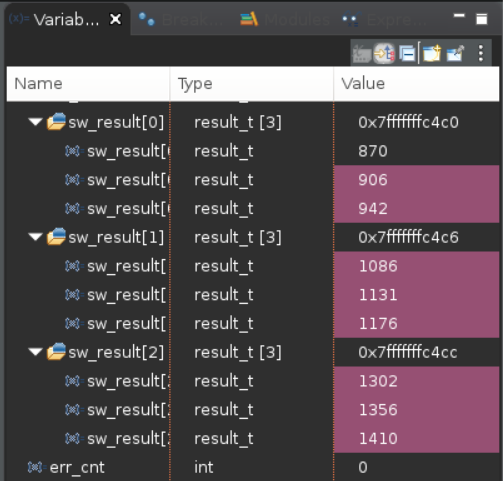
Software computed result
- Click on the Step Into (F5) button to traverse into the matrixmul module, the one that we will synthesize, and observe that the execution is paused on line 37 of the module.
- Using the Step Over (F6) several times, observe the computed results. Once satisfied, you can use the Step Return (F7) button to return from the function.
- The program execution will suspend at line 105 as we had set a breakpoint. Observe the software and hardware (function) computed results in the Variables view.
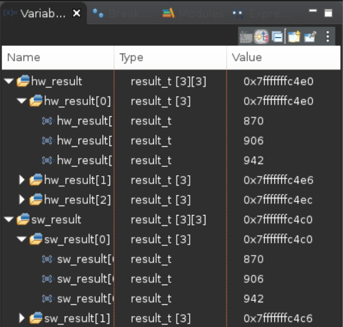
Computed results
- Set a breakpoint on line 96 (return err_cnt;), and click on the Resume button. The execution will continue until the breakpoint is encountered. The console window will show the results as seen earlier (Figure 7).
- Press the Resume button or Terminate button to finish the debugging session.
Synthesize the Design
Switch to Synthesis view and synthesize the design with the defaults. View the synthesis results and answer the question listed in the detailed section of this step.
- Switch to the Synthesis view by clicking Exit Debug button.
- Select Solution > Run C Synthesis > Active Solution to start the synthesis process.
- When the synthesis process is completed, the synthesis results will be displayed along with the Outline pane. Using the Outline pane, one can navigate to any part of the report with a simple click.
Report view after synthesis is completed
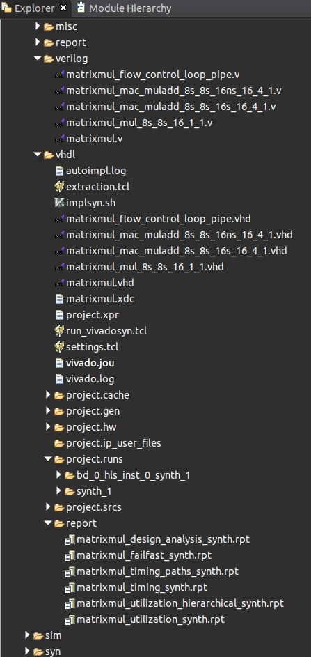
- If you expand solution1 in Explorer, several generated files including report files will become accessible.
Explorer view after the synthesis process
Note that when the syn folder under the Solution1 folder is expanded in the Explorer view, it will show report, verilog, and vhdl sub-folders under which report files, and generated source (vhdl, verilog, header, and cpp) files. By double-clicking any of these entries one can open the corresponding file in the information pane.
Also note that if the target design has hierarchical functions, reports corresponding to lower-level functions are also created.
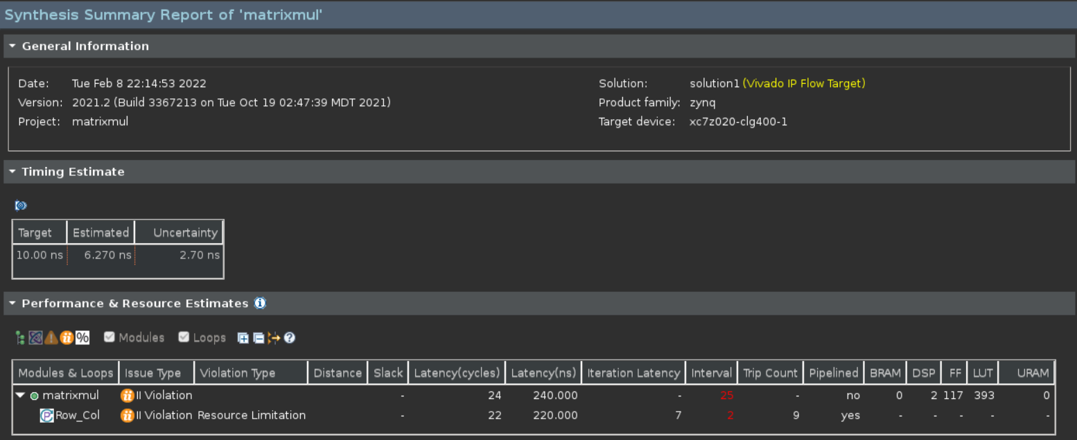
- The Synthesis Report shows the performance and resource estimates as well as estimated latency in the design.
-
Using scroll bar on the right, scroll down into the report and answer the following question.
Question 1 Answer the following question:
Estimated clock period:
Worst case latency:
Number of DSP48E used:
Number of FFs used:
Number of LUTs used: - The report also shows the top-level interface signals generated by the tools.
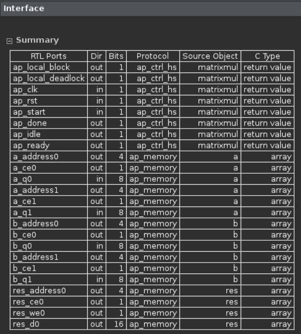
Generated interface signals
You can see ap_clk, ap_rst, ap_ idle and ap_ready control signals are automatically added to the design by default. These signals are used as handshaking signals to indicate when the design is ready to take the next computation command (ap_ready), when the next computation is started (ap_start), and when the computation is completed (ap_done). Other signals are generated based on the input and output signals in the design and their default or specified interfaces.
Analyze using Analysis Perspective
Switch to the Analysis Perspective and understand the design behavior.
-
Select Solution > Open Schedule Viewer or click on Analysis button on tools bar to open the analysis viewer.
The Analysis perspective consists of 4 panes as shown below. Note that the module and loops hierarchies are displayed unexpanded by default. The Module Hierarchy pane shows both the performance and area information for the entire design and can be used to navigate through the hierarchy. The Performance Profile pane is visible and shows the performance details for this level of hierarchy. The information in these two panes is similar to the information reviewed earlier in the synthesis report. The Schedule Viewer is also shown in the right-hand side pane. This view shows how the operations in this particular block are scheduled into clock cycles.
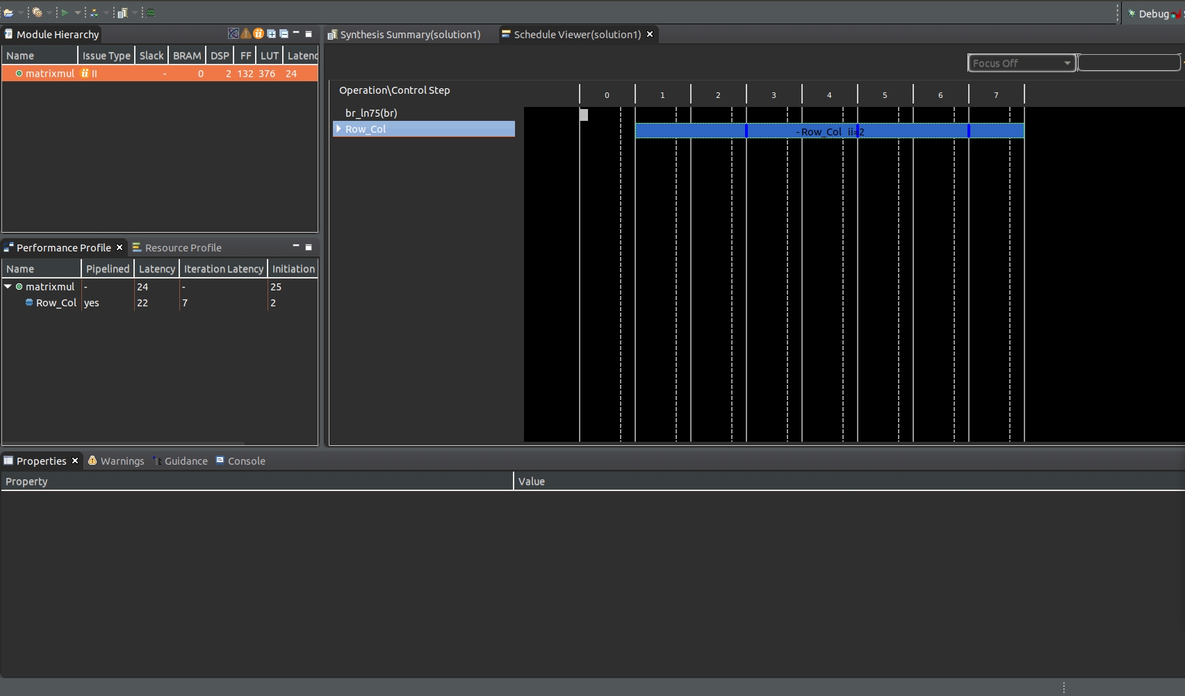
Analysis perspective
- Click on > of loop Row_Col to expand.
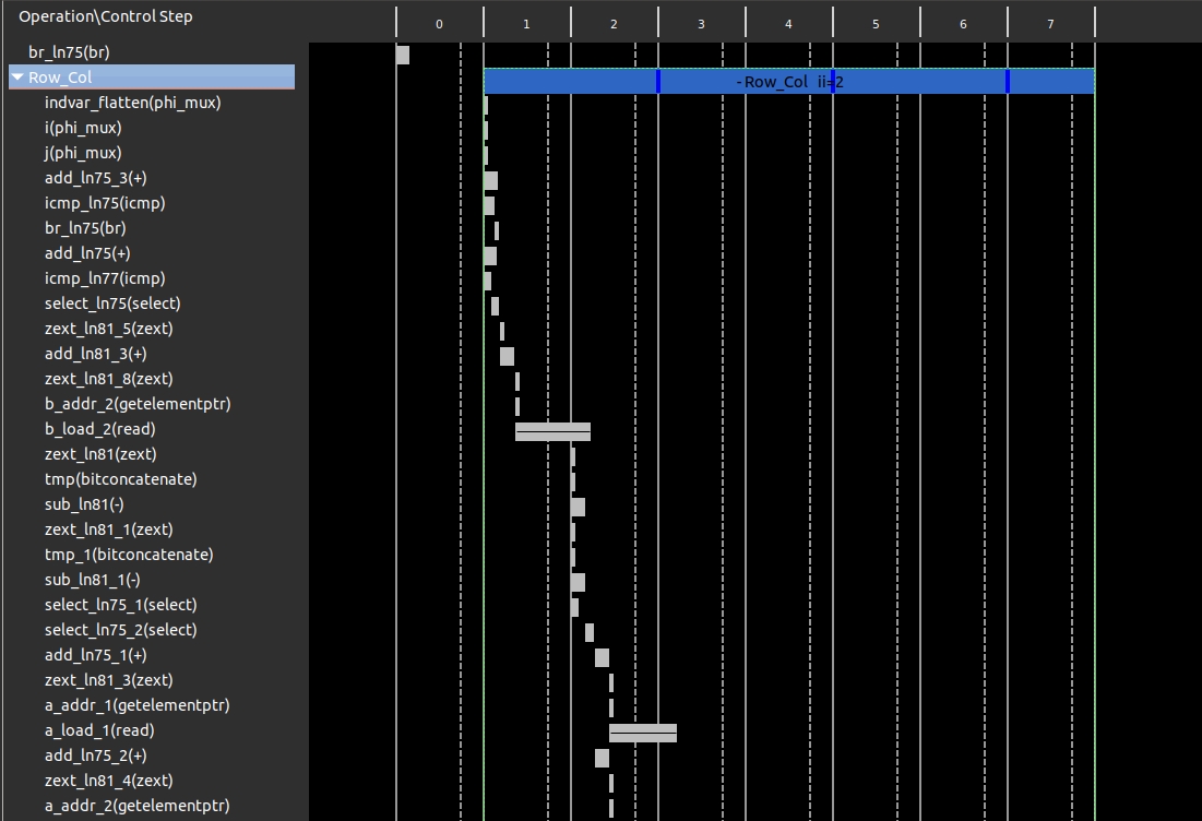
Performance matrix showing top-level Row operation
From this we can see that there is an add operation performed. This addition is likely the counter to count the loop iterations, and we can confirm this.
- Select the block for the adder ( add_in75_3(+)), right-click and select Goto Source.
The source code pane will be opened, highlighting line 37 where the loop index is being tested and incremented.
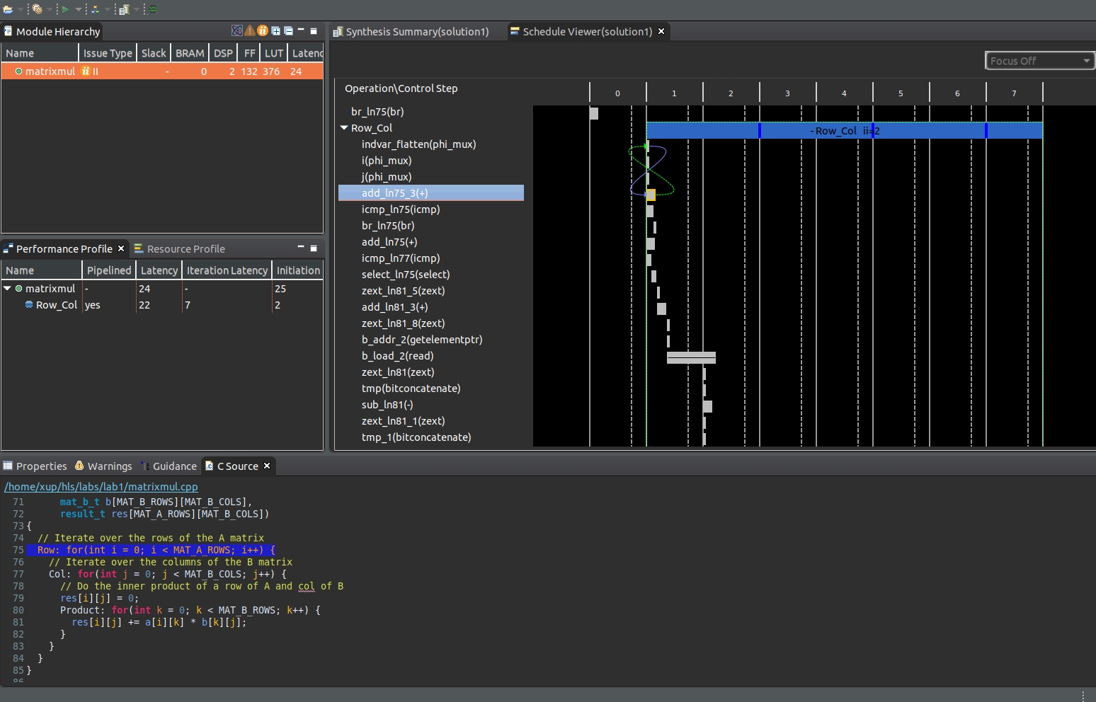
Cross probing into the source file
- Click on the Synthesis tool bar button to switch back to the Synthesis view.
Run C/RTL Co-simulation
Run the C/RTL Co-simulation with the default settings of VHDL. Verify that the simulation passes.
- Select Solution > Run C/RTL Cosimulation to open the dialog box so the desired simulations can be selected and run. A C/RTL Co-simulation Dialog box will open.
- Make sure the VHDL option is selected.
This allows the simulation to be performed using VHDL generated model. To perform the verification using Verilog, you can select Verilog.
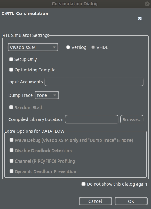
A C/RTL Co-simulation Dialog
-
Click OK to run the VHDL simulation. The C/RTL Co-simulation will run, generating and compiling several files, and then simulating the design. It goes through three stages. First, the VHDL test bench is executed to generate input stimuli for the RTL design.
Second, an RTL test bench with newly generated input stimuli is created and the RTL simulation is then performed.
Finally, the output from the RTL is re-applied to the VHDL test bench to check the results. In the console window you can see the progress and also a message that the test is passed.
This eliminates writing a separate testbench for the synthesized design.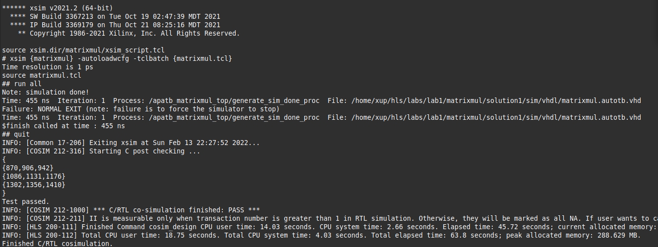
Console view showing simulation progress
-
Once the simulation verification is completed, the simulation report tab will open showing the results. The report indicates if the simulation passed or failed. In addition, the report indicates the measured latency and interval. Since we have selected only VHDL, the result shows the latencies and interval (initiation) which indicates after how many clock cycles later the next input can be provided.
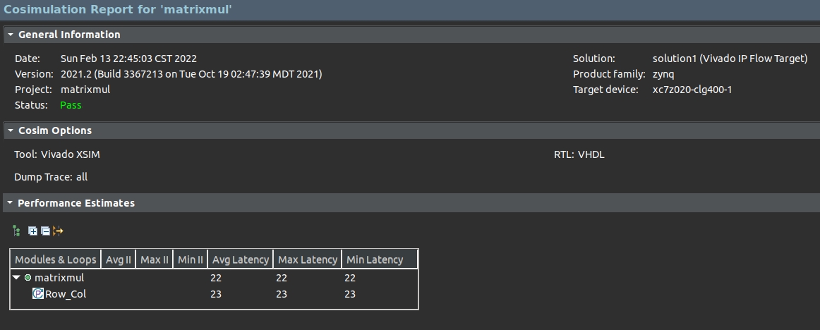
Co-simulation results
Viewing Simulation Results in Vivado
Run Verilog simulation with Dump Trace option selected.
- Select Solution > Run C/RTL Co-simulation to open the dialog box so the desired simulations can be run.
-
Click on the Verilog selection option.
Optionally, you can click on the drop-down button and select the desired simulator from the available list of Vivado XSim, ModelSim, Xcelium, VCS, and Riviera.
- Select All for the Dump Trace option and click OK.
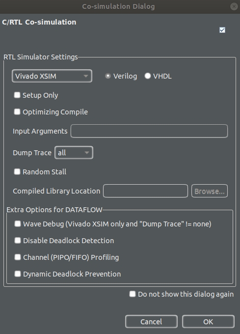
Setting up for Verilog simulation and dump trace
When RTL verification completes, the co-simulation report automatically opens showing the Verilog simulation has passed (and the measured latency and interval). In addition, because the Dump Trace option was used and Verilog was selected, two trace files entries can be seen in the Verilog simulation directory.
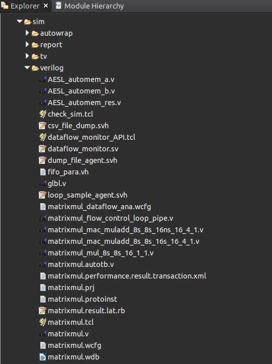
Explorer view after the Verilog RTL co-simulation run
The Co-simulation report shows the test was passed for Verilog along with latency and Interval results.
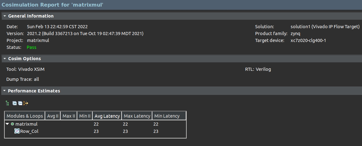
Cosimulation report
Analyze the dumped traces.
- Click on the
 button on tools bar to open the wave viewer. This will start Vivado 2021.2 and open the wave viewer.
 - Click on the zoom fit tool button ( ) to see the entire simulation of one iteration.
- Select a_address0 in the waveform window, right-click and select Radix > Unsigned Decimal. Similarly, do the same for b_address0, a_address1, b_address1 and res_address0 signals.
- Similarly, set the a_q0, b_q0, a_q1, b_q1 and res_d0 radix to Signed Decimal.
You should see the output similar to shown below.
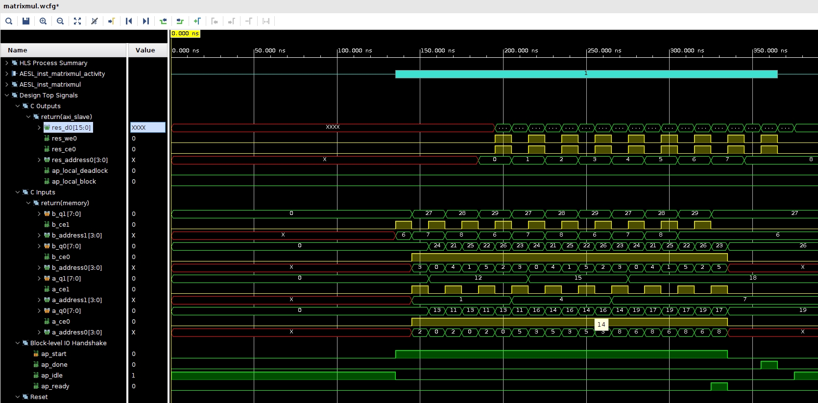
Full waveform showing iteration worth simulation
Note that as soon as ap_start is asserted, ap_idle has been de-asserted indicating that the design is in computation mode. The ap_idle signal remains de-asserted until ap_done is asserted, indicating completion of the process. This indicates 24 clock cycles latency.
- View various part of the simulation and try to understand how the design works.
- When done, close Vivado by selecting File > Exit. Click OK if prompted, and then Discard to close the program without saving.
Export RTL and Implement
In Vitis HLS, export the design, selecting VHDL as a language, and run the implementation by selecting Evaluate option.
- In Vitis HLS, select Solution > Export RTL to open the dialog box.
An Export RTL Dialog box will open.
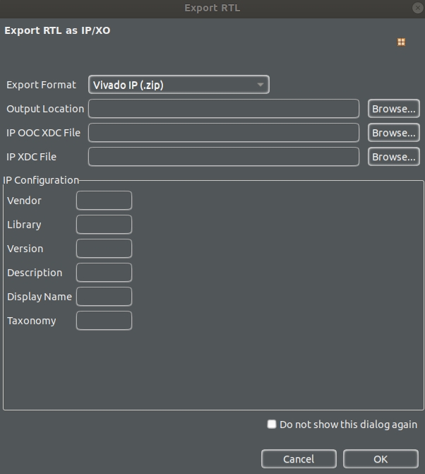
A Export RTL Dialog box
With default settings (shown above), the IP packaging process will run and create a package for the Vivado IP Catalog. Another option available from the Export Format drop-down menu, is to create a Vivado IP for System Generator.
- Select Solution > Implementation to open the dialog box..
- Click on the drop-down menu of the RTL field and select VHDL.
- Click on the RTL Synthesis, Place & Route check box to run the implementation tool.
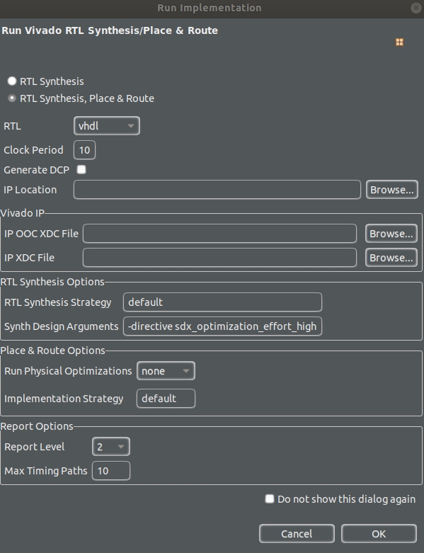
Selecting Evaluate options
-
Click OK and the implementation run will begin.
You can observe the progress in the Vitis HLS Console window. It goes through several phases:
- Exporting RTL as an IP in the IP-XACT format
- RTL evaluation, since we selected Evaluate option, it goes through Synthesis and then through Placement and Routing
Console view
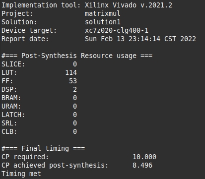
When the run is completed the implementation report will be displayed in the information pane.
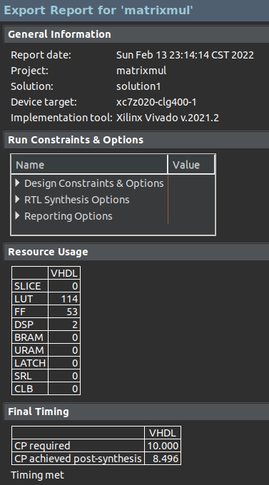
Implementation results in Vitis HLS
Observe that the timing constraint was met, the achieved period, and the type and amount of resources used.
Explorer view after the RTL Export run
-
Expand the Verilog and vhdl sub-folders and observe that the Verilog sub-folder only has the rtl file whereas the vhdl sub-folder has several files and sub-folders as the synthesis and implementation runs were made for it.
It includes project.xpr file (the Vivado project file), matrixmul.xdc file (timing constraint file), project.runs folder among others.
The implementation directory
- Expand the ip folder and observe the IP packaged as a zip file, xilinx_com_hls_matrixmul_1_0.zip, which can be added to the Vivado IP catalog.
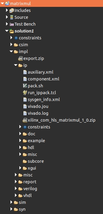
The ip folder content
- Close Vitis HLS by selecting File > Exit.
Conclusion
In this lab, you completed the major steps of the high-level synthesis design flow using Vitis HLS. You created a project, adding source files, synthesized the design, simulated the design, and implemented the design. You also learned how to use the Analysis capability to understand the scheduling and binding.
Answers
Answers for question 1:
Estimated clock period: 6.816 ns
Worst case latency: 24 clock cycles
Number of DSP48E used: 2
Number of FFs used: 66
Number of LUTs used: 365
——————————————————
Copyright© 2022, Advanced Micro Devices, Inc.