HLS Design Flow – System Integration Lab
Introduction
This lab illustrates the HLS design flow for generating IP from the Vitis™ HLS tool. The generated IP is then used to create a subsystem with the Arm® processor from a Zynq® UltraScale+™ MPSoC using the Vivado® IP integrator. The hardware from the Vivado Design Suite is imported into the Vitis environment, and the FIR application is then run on the PYNQ-ZU development board.
Objectives
After completing this lab, you will be able to:
- Describe the HLS design flow to generate the Vivado IP design in Vitis HLS
- Identify the steps and directives involved in creating an IP within the Vitis HLS tool
- Create a system with the Arm processor from a Zynq UltraScale+ MPSoC and IP (fir filter) created with the Vitis HLS tool using the Vivado IP integrator flow
- Use a software application development flow to create and run the application on a development board
The design
The design consists of a FIR filter to filter a 4 KHz tone added to CD quality (48 KHz) music. The characteristic of the filter is as follows: FS=48000 Hz FPASS1=2000 Hz FSTOP1=3800 Hz FSTOP2=4200 Hz FPASS2=6000 Hz APASS1=APASS2=1 dB ASTOP=60 dB This lab requires you to develop a peripheral core of the designed filter that can be instantiated in a processor system. The processor system will acquire a stereo music stream using an on-board CODEC chip and I2C controller, process it through the designed filter (bandstop filter), and output back to the headphone.
Steps
Downdload the audio ctrl IP
Download the audio ctrl IP from https://github.com/Xilinx/PYNQ/tree/master/boards/ip/audio_codec_ctrl_v1.0/src, and put these 10 files into the {labs}/lab4/ip_repo/zed_audio_ctrl/zed_audio_ctrl.srcs/sources_1/imports/i2s_audio folder.
Create a New Project
Create a new project in Vitis HLS targeting xczu5eg-sfvc784-1-e device
- Invoke Vitis HLS Command prompt by selecting Start > Xilinx Design Tools > Vitis HLS 2021.2 Command Prompt then type vitis_hls in the terminal. A Getting Started GUI will appear.
- In the Getting Started section, click on Create Project. The New Vitis HLS Project wizard opens.
- Click Browse… button of the Location field, browse to {labs}/lab4, and then click OK.
- For Project Name, type fir and click Next.
- In the Add/Remove Files for the source files, type fir as the function name (the provided source file contains the function, to be synthesized, called fir).
- Click the Add Files… button, select fir.c and fir_coef.dat files from the {labs}/lab4 folder, and then click Open.
- Click Next.
- In the Add/Remove Testbench Files for the testbench, click the Add Files… button, select fir_test.c file from the {labs}/lab4 folder and click Open.
- Click Next.
- In the Solution Configuration page, leave Solution Name field as solution1 and make sure the clock period as 10. Leave Uncertainty field blank.
- Click on the Part’s Browse button and using the Parts Specify option, select xczu5eg-sfvc784-1-e.
-
Click Finish.
You will see the created project in the Explorer view. Expand various sub-folders to see the entries under each sub-folder.
-
Double-click on the fir.c under the source folder to open its content in the information pane.

The design under consideration
The FIR filter expects x as a sample input and pointer to the computed sample out y. Both of them are defined of data type data_t. The coefficients are loaded in array c of type coef_t from the file called fir_coef.dat located in the current directory. The sequential algorithm is applied and accumulated value (sample out) is computed in variable acc of type acc_t.
-
Double-click on the fir.h in the outline tab to open its content in the information pane.
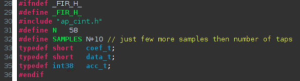
The header file
The header file includes ap_cint.h so user defined data width (of arbitrary precision) can be used. It also defines number of taps (N), number of samples to be generated (in the testbench), and data types coef_t, data_t, and acc_t. The coef_t and data_t are short (16 bits). Since the algorithm iterates (multiply and accumulate) over 59 taps, there is a possibility of bit growth of 6 bits and hence acc_t is defined as int38. Since the acc_t is bigger than sample and coefficient width, they have to cast before being used (like in lines 16, 18, and 21 of fir.c).
-
Double-click on the fir_test.c under the testbench folder to open its content in the information pane.
Notice that the testbench opens fir_impulse.dat in write mode, and sends an impulse (first sample being 0x8000).
Run C Simulation
Run C simulation to observe the expected output.
- Select Project > Run C Simulation or click on the button from the tools bar buttons, and click OK in the C Simulation Dialog window.
The testbench will be compiled using apcc compiler and csim.exe file will be generated. The csim.exe will then be executed and the output will be displayed in the console view.
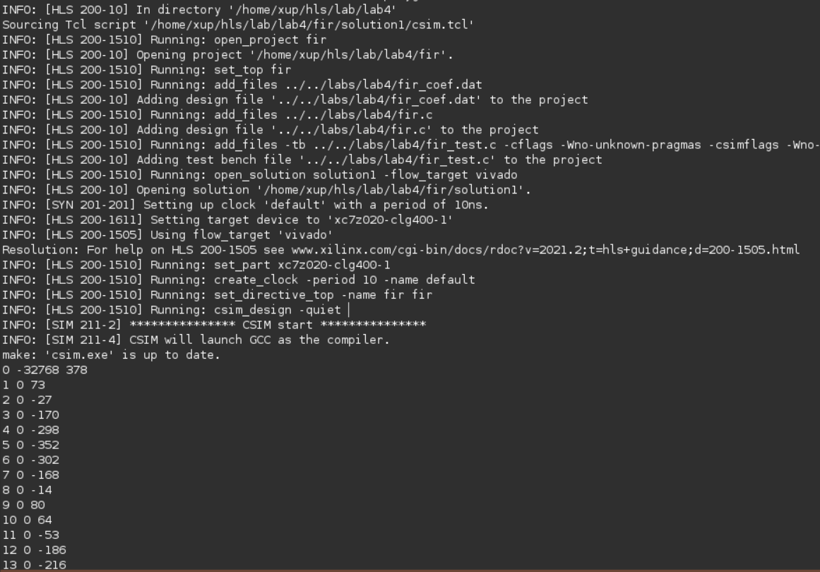
Initial part of the generated output in the Console view
You should see the filter coefficients being computed.
Synthesize the Design with the defaults
Synthesize the design with the defaults. View the synthesis results and answer the question listed in the detailed section of this step.
- Select Solution > Run C Synthesis > Active Solution to start the synthesis process.
- When synthesis is completed, several report files will become accessible and the Synthesis. Results will be displayed in the information pane.
- The Synthesis Report shows the performance and resource estimates as well as estimated latency in the design.
- Using scroll bar on the right, scroll down into the report and answer the following question.Question 1Estimated clock period:Worst case latency:Number of DSP48E used:Number of BRAMs used:Number of FFs used:Number of LUTs used:
- The report also shows the top-level interface signals generated by the tools.
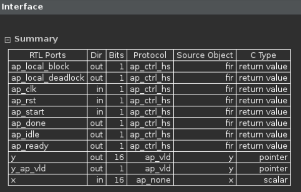
Generated interface signals
You can see the design expects x input as 16-bit scalar and outputs y via pointer of the 16-bit data. It also has ap_vld signal to indicate when the result is valid.
Run RTL/C CoSimulation
Run the RTL/C Co-simulation, selecting Verilog. Verify that the simulation passes.
- Select Solution > Run C/RTL Co-simulation to open the dialog box so the desired simulations can be run.
-
Select the Verilog option and click OK.
The Co-simulation will run, generating and compiling several files, and then simulating the design. In the console window you can see the progress. When done the RTL Simulation Report shows that it was successful and the latency reported was 68.
Setting Up the AXI Lite Adapters and Re-synthesizing the Design
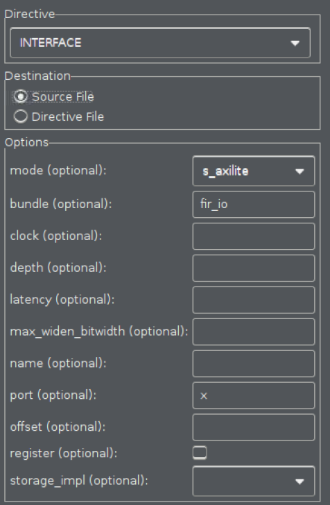
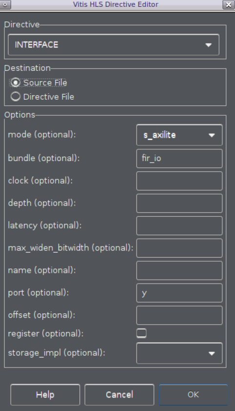
Add INTERFACE directive to create AXI4LiteS adapters so IP-XACdT adapter can be generated during the RTL Export step.
- Make sure that fir.c file is open and in focus in the information view.
- Select the Directive tab.
- Right-click x, and click on Insert Directive….
- In the Vitis HLS Directive Editor dialog box, select INTERFACE using the drop-down button.
- Click on the button beside mode (optional). Select s_axilite.
-
In the bundle (optional) field, enter fir_io and click OK.
Selecting the AXI4LiteS adapter and naming bundle
-
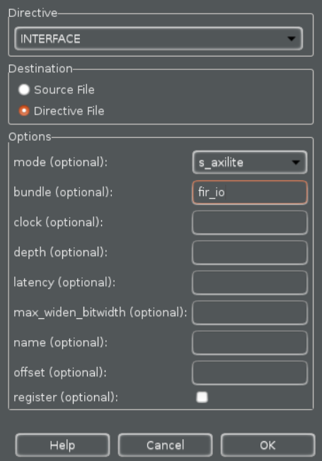
Similarly, apply the INTERFACE directive (including bundle) to the y output.
Applying bundle to assign y output to AXI4Lite adapter
-
Apply the INTERFACE directive to the top-level module fir to include ap_start, ap_done, and ap_idle signals as part of bus adapter (the variable name shown will be return). Include the bundle information too. There is a bug in the tool, as it does not update the directives.tcl file with this directive.
Applying bundle to assign function control signals to AXI4Lite adapter
Note that the above steps will create address maps for x, y, ap_start ap_valid, ap_done, and ap_idle, which can be accessed via software. Alternately, ap_start, ap_valid, ap_done, ap_idle signals can be generated as separate ports on the core. These ports will then have to be connected in a processor system using available GPIO IP.
-
Worksaround for this bug is to modify the source code and apply using pragma. Enter the following line on line number 11.
#pragma HLS INTERFACE s_axilite port=return bundle=fir_io
Save the file.
Re-synthesize the design
Re-synthesize the design as directives have been added. Run the RTL Export to export the design as an IP.
-
Since the directives have been added, it is necessary to re-synthesize the design. Select Solution > Run C Synthesis > Active Solution.
Check the Interface summary at the bottom of the Synthesis report to see the interface that has been created.
-
Once the design is synthesized, select Solution > Export RTL to open the dialog box so the desired IP can be generated. An Export RTL Dialog box will open.
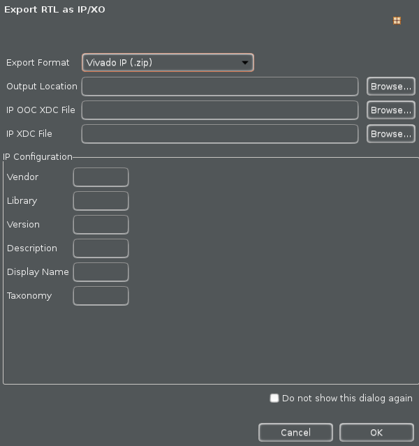
Export RTL Dialog
- Click OK to export the design as an IP.
-
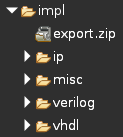
When the run is completed, expand the impl folder in the Explorer view and observe various generated directories, such as ip, misc, verilog and vhdl.
IP-XACT adapter generated
Expand the ip directory and observe several files and sub-directories. One of the sub-directory of interest is the drivers directory which consists of header, c, tcl, mdd, and makefile files. Another file of interest is the zip file, which is the ip repository file that can be imported in an IP Integrator design
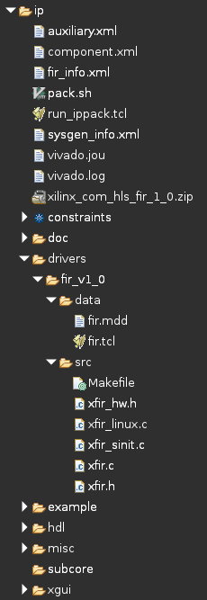
Adapter’s drivers directory
- Close Vitis HLS by selecting File > Exit.
Create a Vivado Project
Open a terminal and run the provided tcl script to create an initial system targeting the PYNQ-ZU board.
- Download the board files of PYNQ-ZU from /board_files, and put it in the folder **
/data/xhub/boards/XilinxBoardStore/boards/Xilinx/** on Linux, while ** \\data\\xhub\\boards\\XilinxBoardStore\\boards\\Xilinx\\** on Windows, where ** ** should be replaced by the install_path on your computer. - On Linux machine, open a terminal directly. While on Windows machine, open a Command Prompt window.
- Execute **source
/settings64.sh** on Linux, while ** \\settings64-Vivado.bat** on Windows, where ** ** should be replaced by the install_path on your computer. - Change the directory to {labs}/lab4 using the cd command.
-
Run the provided script file to create an initial system having zed_audio_ctrl and GPIO peripherals by typing the following command:
vivado -source pynq_zu_audio_project_create.tcl
The script will be run and the initial system, shown below, will be created.
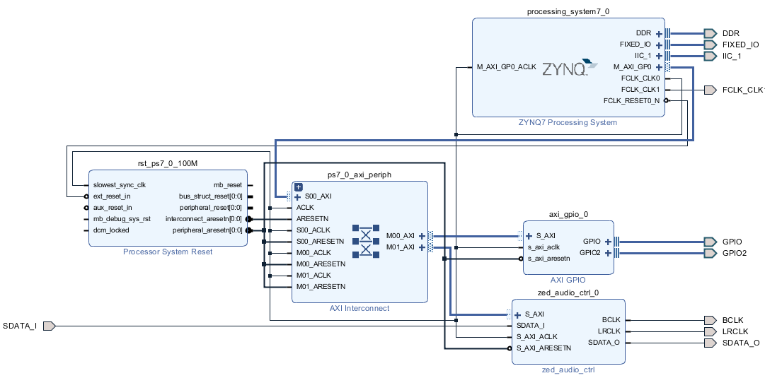
Block design made for Pynq
Add the HLS IP to the IP Catalog
- Select Flow Navigator > Project Manager > Settings
- Expand IP > Repository in the left pane.
-
Click the + button (The lab4/ip_repo directory has already been added). Browse to {labs}/lab4/fir/solution1/impl/ip and click Select.
The directory will be scanned and added in the IP Repositories window, and one IP entry will be detected.
-
Click OK.
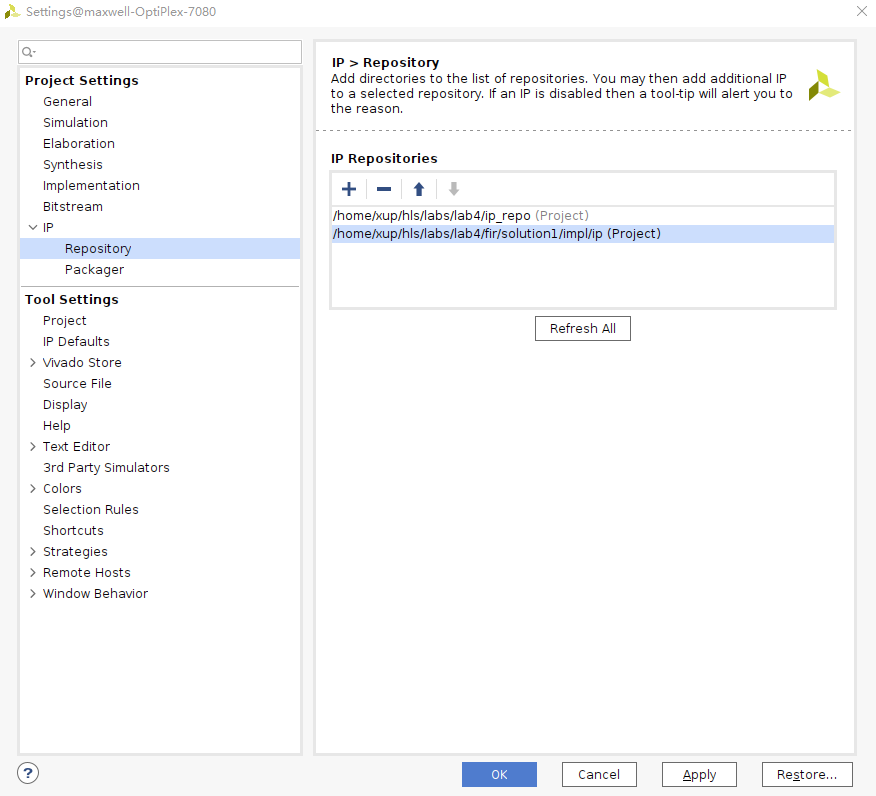
Setting path to IP Repositories
- Click OK to accept the settings.
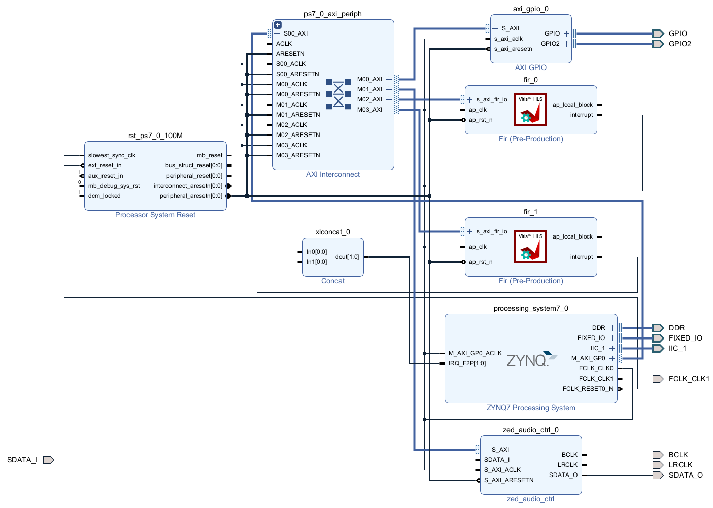
Instantiate fir_top core twice, one for each channel, into the processing system.
- Click the Add IP icon (plus sign icon) and search for Fir in the catalog by typing Fir and double-click on the Fir entry to add an instance. Notice that the added IP has HLS logo in it indicating that this was created by Vitis HLS.
- Similarly, add another instance of the HLS IP.
- Click on Run Connection Automation, and select All Automation.
- Click on /fir_0/s_axi_fir_io and /fir_1/ s_axi_fir_io. and verify that they will both be connected to the M_AXI_GP0, and click OK.
Enable the PS-PL Interrupt ports > IRQ_F2P ports. Add an instance of concat IP with two single-bit input ports. Connect input ports to the interrupt ports of the two FIR instances and the output port to the IRQ_F2P port of the processing_system7_0 instance.
- Double-click on the processing_system7_0 instance to open the re-customization form.
- Select the Interrupts entry in the left pane, click on the Fabric Interrupts check box in the right.
- Expand the Fabric Interrupts > PL-PS Interrupt Ports > IRQ_F2P entry in the right, and click the check-box of IRQ_F2P[15:0].
- Click OK.
- Add an instance of the concat IP.
- Connect the interrupt port of each of the FIR instances to the two input ports of the xlconcat_0 instance.
-
Connect the output port of the xlconcat_0 instance to the IRQ_F2P port of the processing_system7_0 instance.
At this stage the design should look like shown below (you may have to click the regenerate button).
Verify addresses and validate the design. Generate the system_wrapper file, and add the provided Xilinx Design Constraints (XDC).
- Click on the Address Editor, and expand the processing_system7_0 > Data if necessary. The generated address map should look like as shown below.
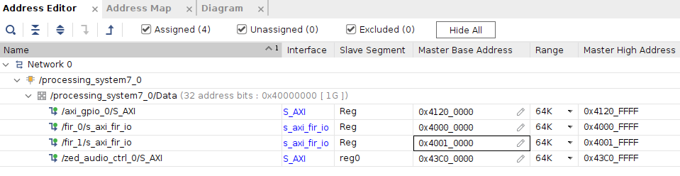
Generated address map
- Run Design Validation (Tools > Validate Design) and verify there are no errors
- In the sources view, right-click on the block diagram file, system.bd, and select Create HDL Wrapper to update the HDL wrapper file. When prompted, click OK with the Let Vivado manage wrapper and auto-update option.
- Click Add Sources in the Flow Navigator pane, select Add or Create Constraints, and click Next.
- Click the Add Files button, browse to the {labs}/lab4 folder, select pynq_zu_audio_constraints.xdc.
- Click Copy constraints files into project and then click Finish to add the file.
- Click on the Generate Bitstream in the Flow Navigator to run the synthesis, implementation, and bitstream generation processes.
- Click Save, Yes, and OK if prompted to start the process.
- When the bit generation is completed, a selection box will be displayed with Open Implemented Design option selected. Click Cancel.
Export to Vitis and create Application Project
Export the hardware along with the generated bitstream to Vitis.
- Select File > Export > Export Hardware…
- Click Next
- Make sure that Include Bitstream option is selected and click OK, leaving the target directory set to local project directory {labs}/lab4/audio.
- Open Vitis 2021.2
- Change the workspace to {labs}/lab4/audio and click Launch
- In Vitis, select File > New > Platform Project
- Enter audio as the Platform project name and click Next
- For XSA File, browse to {labs}/lab4/audio and select system_wrapper.xsa
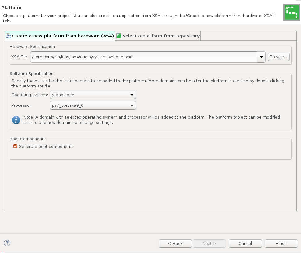
Hardware Specification
- Click Finish with the default settings (with standalone operating system).
- Select File > New > Application Project
- Click Next
- In Select a platform from repository tab, select audio as the platform.
- Click Next
- Enter Test as the Project Name and click Next
- Click Next, select standalone_domain for the domain.
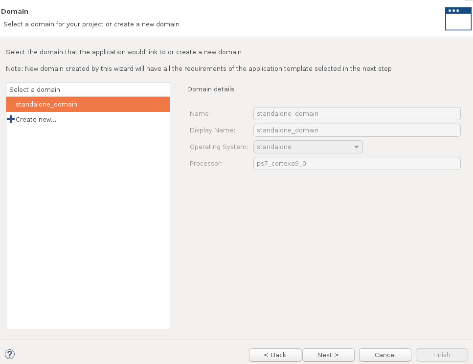
Select domain
- Click Next, select Empty Application(C) and click Finish
- Select Test in the project view, right-click the src folder, and select Import Sources…
- Browse to {labs}/lab4 folder.
- Select both pynq_zu_testapp.c and pynq_zu_audio.h and click Finish to add the files to the project.
- Select Test_system inn the Assistant view, right-click and select Build. The program should compile successfully.
Verify the Design in Hardware
Connect a micro-usb cable between a PC and the JTAG port of the board. Connect an audio patch cable between the Line In jack and the speaker (headphone) out jack of a PC. Connect a headphone to the Line Out jack on the board. Power On the board.
- Connect a micro-usb cable between a PC and the JTAG port of the board.
- Connect an audio patch cable between the Line In jack and the speaker out (headphone) jack of a PC.
- Connect a headphone to the HP+MIC jack on board. Power ON the board.
- Select Xilinx > Program Device.
- Make sure that the system_wrapper.bit bitstream is selected.
- Click Program. This will configure the FPGA.
- Double-click corrupted_music_4KHz.wav or some other wave file of interest to play it using the installed media player. Place it in the continuous play mode.
- Right-click on the Test_system in the Assistant view and select Run > Run configuration.
-
Double-click on the System Project Debug to create the Run configuration, and then click on Run
The program will be downloaded and run. If you want to listen to corrupted signal then set the SW0 OFF. To listened the filtered signal set the SW0 ON.
- When done, power OFF the board.
- Exit Vitis and Vivado using File > Exit.
Conclusion
In this lab, you developed an IP from the C design of a FIR filter using the Vitis HLS tool. Using the Vivado IP integrator, you next created a system with the Arm processor from the Zynq UltraScale+ MPSoC and the FIR IP. You then used a test application to write into and read from the IP interface registers.
Answer
Answers for question 1: Estimated clock period: 1.878 ns Worst case latency: 70 Number of DSP48E used: 3 Number of BRAMs used: 0 Number of FFs used: 237 Number of LUTs used: 257
Appendix
Create a Project using Vivado GUI
Launch Vivado and create an empty project targeting the Pynq-ZU (xczu5eg-sfvc784-1-e)
- Open Vivado 2021.2
- Click Create Project to start the wizard. You will see the New Project dialog box. Click Next.
- Click the Browse button of the Project Location field of the New Project form, browse to {labs}/lab4, and click Select.
- Enter audio in the Project Name field. Make sure that the Create Project Subdirectory box is checked. Click Next.
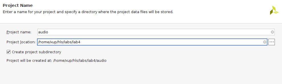
Project Name entry
- Select RTL Project in the Project Type form, and click Next.
- Select Verilog as the Target language in the Add Sources form, and click Next.
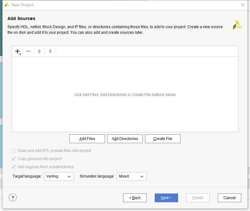
Add sources to new project
- Click Next two times to skip Adding Existing IP and Add Constraints dialog boxes
- In the Default Part form, and select pynq-zu. Click Next.

Boards and Parts selection
- Check the Project Summary and click Finish to create an empty Vivado project.
Creating the System Using the IP Integrator
Use the IP Integrator to create a new Block Design, and generate the ARM Cortex-A9 processor based hardware system.
- In the Flow Navigator, click Create Block Design under IP Integrator
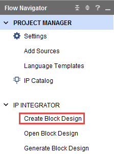
Create IP Integrator Block Diagram
- Enter system for the design name and click OK.
- IP from the catalog can be added in different ways. Click on Add IP in the message at the top of the Diagram panel, or click the Add IP icon in the block diagram side bar, press Ctrl + I, or right-click anywhere in the Diagram workspace and select Add IP.
- Once the IP Catalog is open, type “zy” into the Search bar, find and double click on ZYNQ7 Processing System entry, or click on the entry and hit the Enter key to add it to the design.
The Zynq IP Block
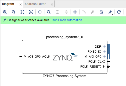
- Notice the message at the top of the Diagram window that Designer Assistance available. Click on Run Block Automation and select /processing_system7_0
- Click OK when prompted to run automation.
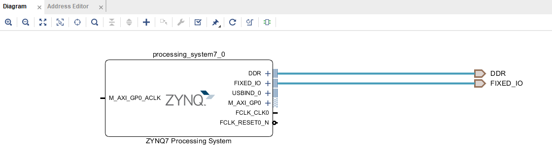
Zynq Block with DDR and Fixed IO ports
- In the block diagram, double click on the Zynq block to open the Customization window for the Zynq processing system. A block diagram of the Zynq should now be open, showing various configurable blocks of the Processing System. At this stage, the designer can click on various configurable blocks (highlighted in green) and change the system configuration.
Configure I/O Peripherals block to use UART 1 and I2C 1 peripherals, disabling other unwanted peripherals. Uncheck Timer 0. Enable FCLK_CLK1, the PL fabric clock and set its frequency to 10.000 MHz for the Pynq
- Select the MIO Configuration tab on the left to open the configuration form and expand I/O Peripheral in the right pane.
- Click on the check box of the I2C 1 peripheral. Uncheck USB0, SD 0, ENET 0, GPIO > GPIO MIO as we don’t need them.
- Expand the Application Processing Unit group in the Select the MIO Configuration tab and uncheck the Timer 0.
- Select the Clock Configuration in the left pane, expand the PL Fabric Clocks entry in the right, and click the check-box of FCLK_CLK1.
- Change the Requested Frequency value of FCLK_CLK1 to 10.000 MHz
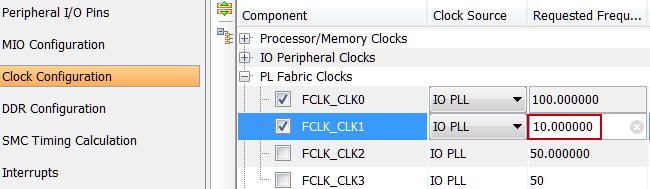
Enabling and setting the frequency of FCLK_CLK1
- Click OK. Notice that the Zynq block only shows the necessary ports.
Add the provided I2C-based IP
- In the Flow Navigator pane, click Settings under Project Manager.
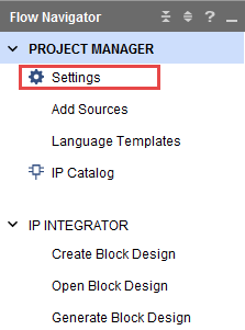
Invoking Project Settings
- Expand IP > Repository in the left pane.
- Click the + button. Browse to {labs}/lab4/ip_repo and click Select. The directory will be scanned and added in the IP Repositories window, and two IP entry will be detected.
- Click OK to accept the settings.
Instantiate zed_audio_ctrl and GPIO with width of 2 bits on channel 1 and width of 1 bit input only on channel 2. Run connection automation to connect them.
- Click the Add IP button if the IP Catalog is not open and search for AXI GPIO in the catalog by typing gpi and double-click on the AXI GPIO entry to add an instance.
- Double-click on the added instance and the Re-Customize IP GUI will be displayed.
- Select IP Configuration.
- Change the GPIO Width to 2.
- Check the Enable Dual Channel box, set the GPIO Width of GPIO 2 to 1 only, and click OK.
- Similarly add an instance of the zed_audio_ctrl.
- Notice that Design assistance is available. Click on Run Connection Automation, and select /axi_gpio_0/S_AXI
- Click OK to connect it to the M_AXI_GP0 interface. Notice two additional blocks, Proc Sys Reset, and AXI Interconnect have automatically been added to the design.
- Similarly, click on Run Connection Automation, and select /zed_audio_ctrl_0/S_AXI.
Make IIC_1, GPIO, FCLK_CLK1, and zed_audio_ctrl ports external.
- Select the GPIO interface of the axi_gpio_0 instance, right-click on it and select Make External to create an external port. This will create the external port named GPIO and connect it to the peripheral.
- Select the GPIO2 interface of the axi_gpio_0 instance, right-click on it and select Make External to create the external port.
- Similarly, selecting one port at a time of the zed_audio_ctrl_0 instance, make them external.
- Similarly, make the IIC_1 interface and FCLK_CLK1 port of the processing_system7_0 instance external.
- Change the names of BCLK_0 to BCLK, LRCLK_0 to LRCLK, SDATA_O_0 to SDATA_O, SDATA_I_0 to SDATA_I, GPIO_0 to GPIO, and GPIO2_0 to GPIO2 to match the signal names useed in the provided design constraint file.
At this stage the design should look like shown below (you may have to click the regenerate layout button).
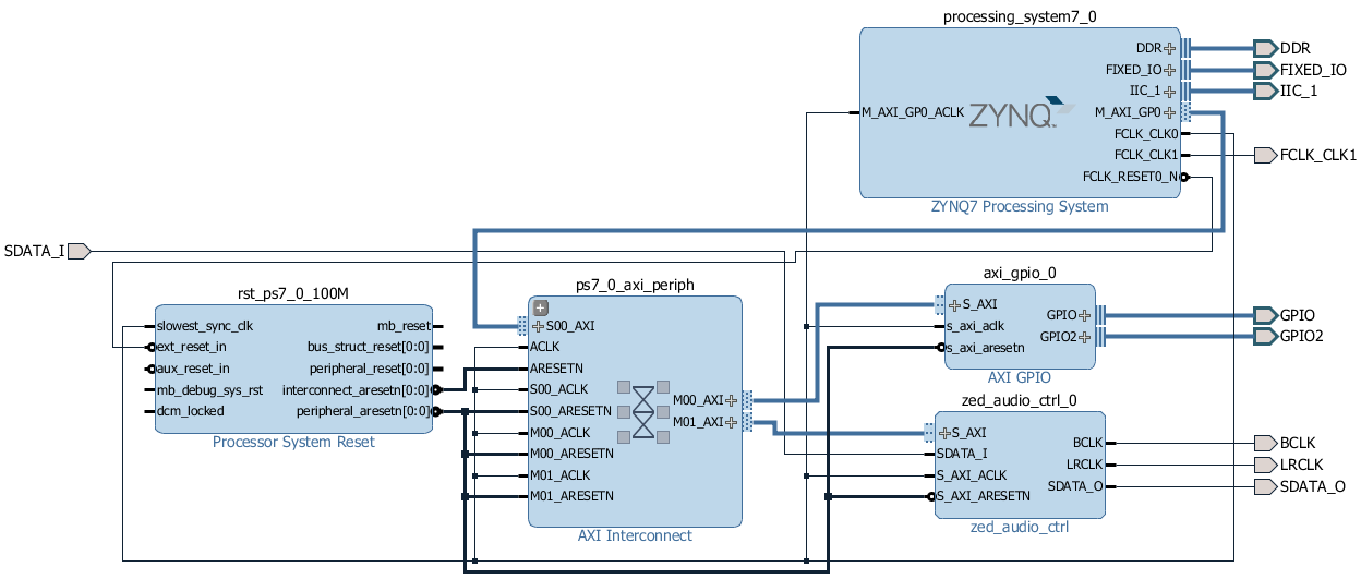
Block design after I2C based zed_audio_ctrl core added and connections made for the Pynq