AIE Test Harness
This repository provides a test harness to help AIE developers easily build and test their AIE graph on both VCK190 and VEK280 devices. This test harness is designed to provide a very simple and intuitive transition from the AIE simulation environment to testing user AIE graph on hardware. With the test harness, AIE graphs running in simulation can be taken to hardware in just a few minutes and with only a few minor modifications required.
Either VCK190 test harness or VEK280 test harness consists of three main parts:
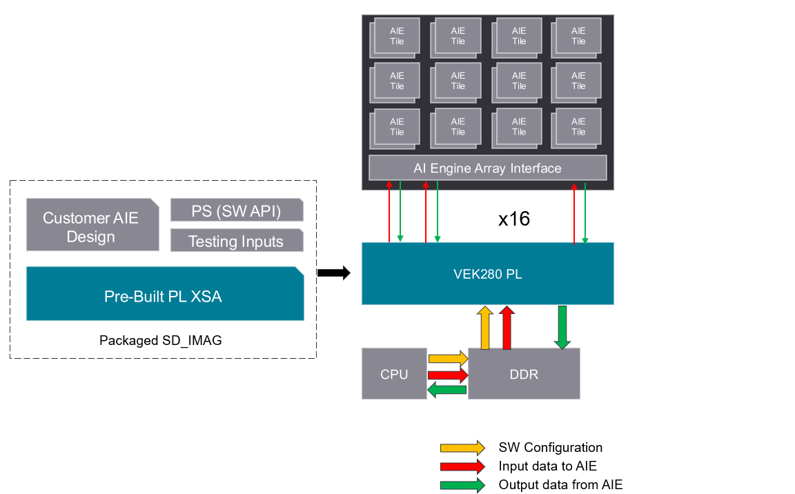
- A precompiled .xsa which has a PL DMA engine to transfer data between DDR and a set of predefined 128-bit AI Engine PLIOs. It is important to be noticed that we have enhanced the VCK190 test harness in this release, where the number of PLIOs are extended from 16x to 36x and the functional testing mode and performance testing mode are supported on this device as well (see system block diagram of VCK190 test harness below). The VEK280 test harness has the same feature as what we have implemented for VCK190 in 2023.1 release (16x PLIOs with limitied test scale performance testing mode only), corresponding system block diagram is shown below.
- A set of software APIs to facilitate the development of the application used to initialize the device, configure the PL DMA engine, and run the tests.
- A set of scripts to easily package the user’s libadf.a and test application, and generate the boot image for harware board-run.

The test harness leverages a precompiled .xsa file which is used as an input platform when compiling the AIE graph (providing necessary hardware information). This allows skipping the v++ link step after compiling the libadf.a and directly go to the v++ package step to generate the hardware boot image. This saves the most time-consuming part of the build process for on-board tests and allows to fast and predictable iterations.
On VCK190, the precompiled .xsa implements a PL DMA engine with 72 independent AXI stream channels. 36 channels send data from DDR to AIE and 36 channels receive data from AIE to DDR. On VEK280, it has 32 independent AXI stream channels that 16 channels can send data from DDR to AIE and 16 channels can receive data from AIE to DDR. For both of the DMA engines, they are designed to allow a maximum throughput on the PLIO interfaces (128-bit @ 312.5MHz), ensuring that the AIE graph isn’t artificially stalled by the DMA channels and thereby allowing accurate performance testing in hardware (except for functional testing mode on VCK190).
The software APIs enable pure AIE designers to easily build SW applications to test an AIE graph using the test harness. The APIs are designed to structure test applications following these 5 simple steps:
- Initialize the device, load the xclbin, and inferring the testing mode
- Configure how each DMA channel transfers data to or from the AIE graph
- Run the AIE graph as well as the PL data mover
- Wait for all the data to be sent/received
- Check correctness of results (correctness of result is not guaranteed when test scale is lager than URAM capacity in each channel on VCK190) and do profiling on performance testing modes for each channel