Design Example 1: Using GPIOs, Timers, and Interrupts
The Zynq® UltraScale+™ MPSoC ZCU102 evaluation board comes with a few configurable switches and LEDs. This design example makes use of bare-metal and Linux applications to toggle these LEDs, with the following details:
The Linux APU runs Linux, while the RPU R5-0 hosts another bare-metal application.
The Linux applications configure a set of PL LEDs to toggle using a PS dip switch, and another set of PL LEDs to toggle using a PL Dip Switch (SW17).
The R5-Core 0 application uses an AXI Timer IP in the programmable logic to toggle PS LED (DS50). The application is configured to toggle the LED state every time the timer counter expires, and the timer in the PL is set to reset periodically after a configurable time interval.
The system is configured so that the APU Linux application and RPU bare-metal application run simultaneously.
Configuring Hardware
The first step in this design is to configure the PS and PL sections. This can be done in Vivado® IP integrator. Start with adding the required IPs from the Vivado IP catalog, and then connect the components to blocks in the PS subsystem.
If the Vivado Design Suite is already open, start from the block diagram shown in and jump to step 4.
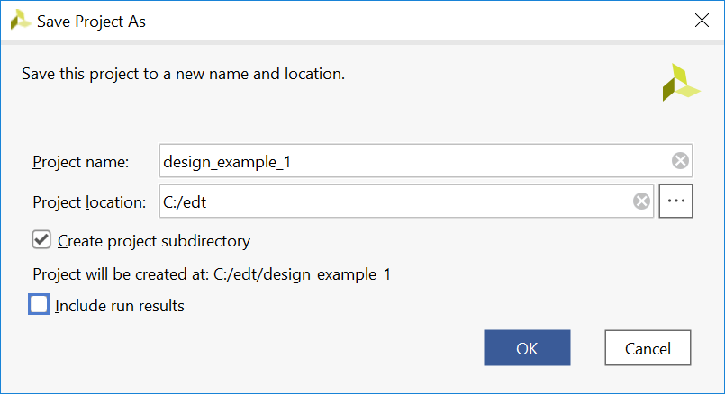
Open the Vivado project that you created in the introduction tutorial:
C:/edt/edt_zcu102/edt_zcu102.xprSave the project as
design_example_1:Click File → Project → Save As.
Input project name design_example_1.
Deselect Include run results.
Click OK.
In the Flow Navigator, under IP integrator, click Open Block Design and select
edt_zcu102.bd.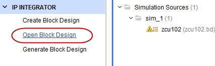
Adding the AXI Timer and AXI GPIO IP
Adding the AXI Timer IP:
Right-click in the block diagram and select Add IP from the IP catalog.
In the catalog, select AXI Timer. The IP Details information displays, as shown in the following figure.
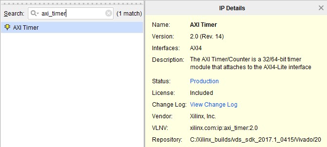
Double-click the AXI Timer IP to add it to the design.
Review the AXI Timer configurations:
Double-click the AXI Timer IP block to configure the IP, as shown in following figure.
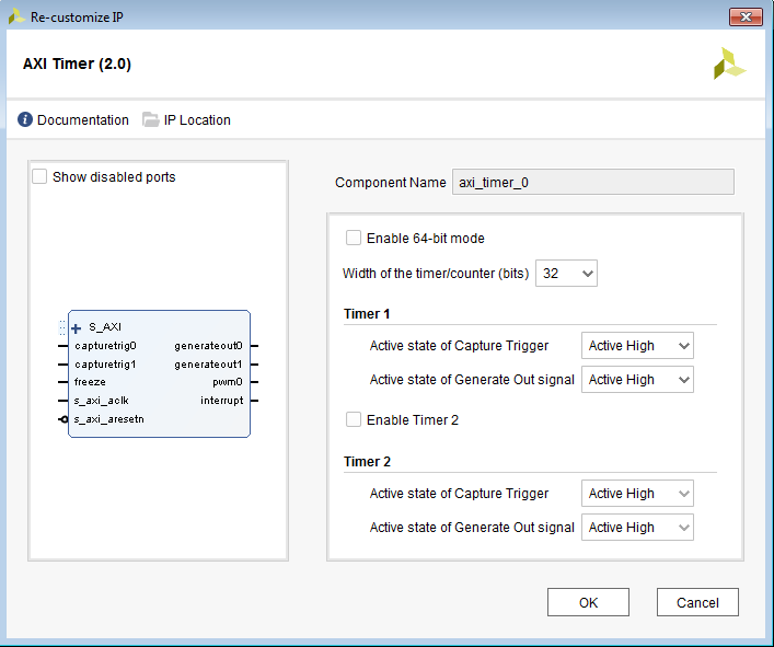
Click OK to close the window.
Add the AXI GPIO IP:
Right-click in the block diagram and select Add IP.
Search for “AXI GPIO” and double-click the AXI GPIO IP to add it to the design.
Add the second AXI GPIO IP:
Copy the axi_gpio_0 IP by typing Ctrl+C.
Paste it by typing Ctrl+V.
You can see that axi_gpio_1 is created.
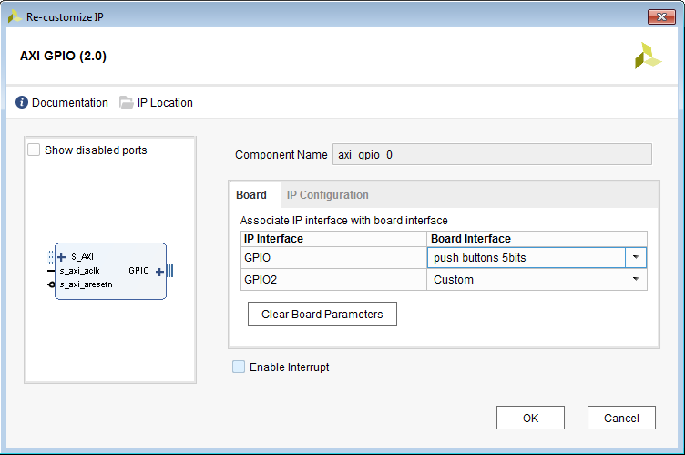
Configure axi_gpio_0 for push buttons:
Double-click axi_gpio_0 to open its configurations.
Select Push button 5bits from the Board Interface drop-down list on the GPIO row.
Click OK.
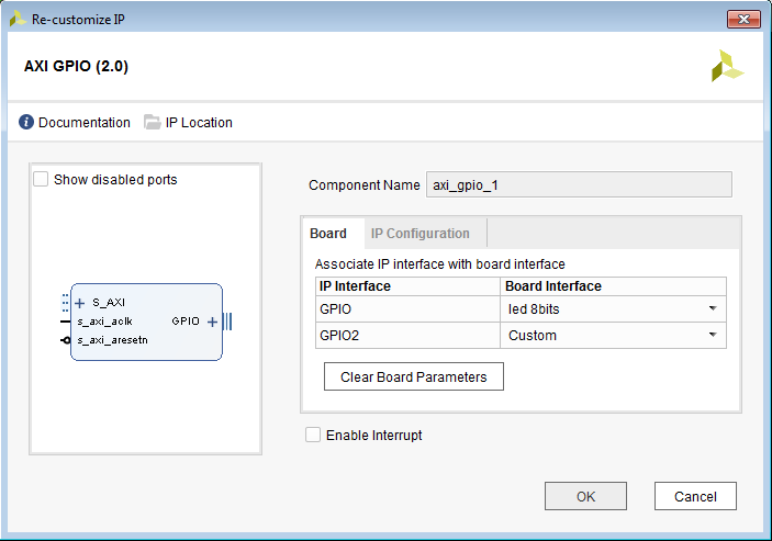
Configure axi_gpio_1 for PL LEDs:
Double-click axi_gpio_1 to open its configurations.
Select led_8bits from the Board Interface drop-down list on the GPIO row.
Click OK.
Connecting IP Blocks to Create a Complete System
The next step is to connect the IP blocks instantiated above to the PS block.
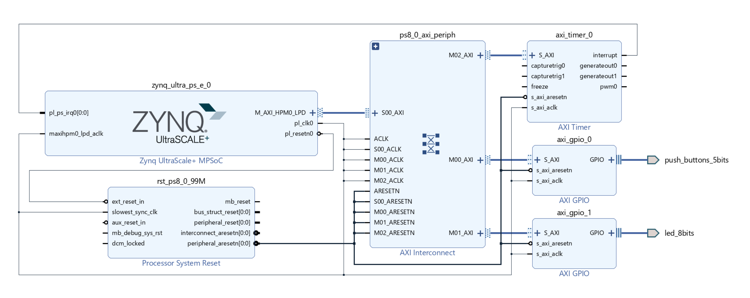
Use PS HPM LPD AXI to control the AXI interface of the GPIO and timer.
Connect interrupt signals.
Enable the PS AXI HPM LPD AXI interface:
Double-click the Zynq UltraScale+ MPSoC IP block.
Select the PS-PL Configuration tab.
Enable AXI HPM0 LPD, expand it, and set the AXI HPM0 LPD Data Width drop-down to 32 bits.
Click OK to close the window.
Check that the M_AXI_HPM0_LPD interface shows up on the MPSoC block.
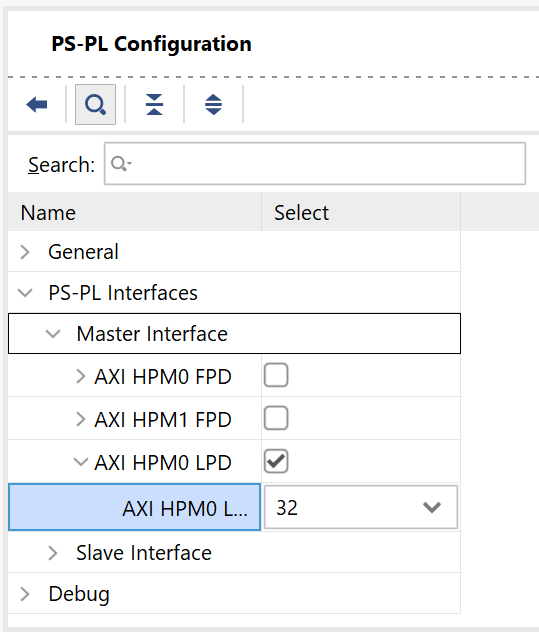
Note: 32-bit AXI is useful for accessing the control registers of general IPs. 128-bit AXI is useful for data transfer.
Connect the AXI interfaces:
Click Run Connection Automation.
Check All Automation.
Go through each tab to review the planning connections.
Click OK to execute the automated connection.
Check the connection result.
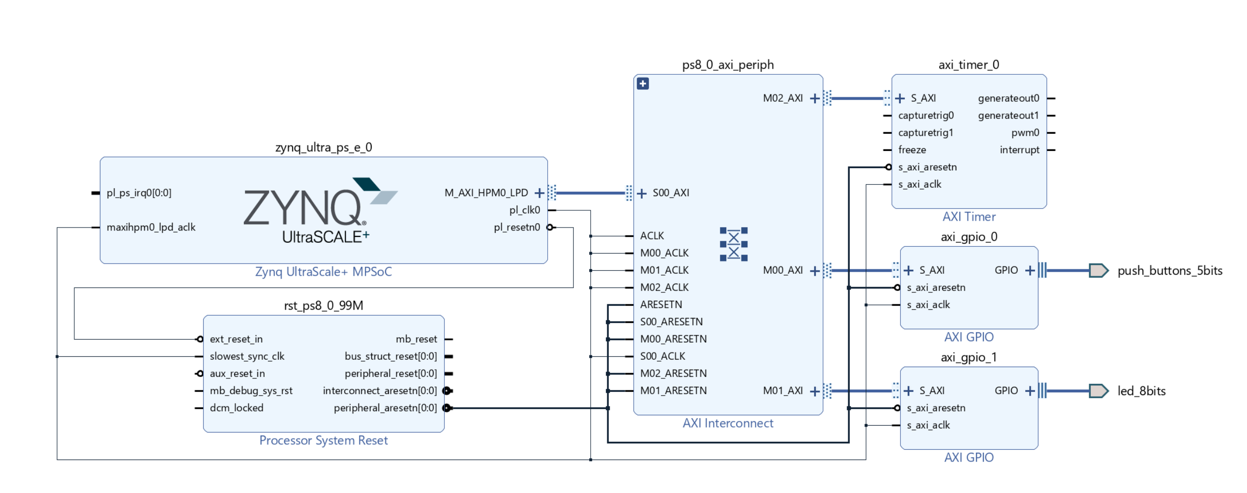
Connect the interrupt signals:
Connect axi_timer_0.interrupt to zynq_ultra_ps_e_0.pl_ps_irq0[0:0].
The AXI GPIO interrupt mode will not be used.
Review the final block diagram.
Note: If you have multiple interrupt signals to connect to the PS, you can concatenate them to a bus with a
concatblock. You can addconcatfrom Add IP.Verify the address settings of IP cores:
In the Address Editor view, verify that the corresponding IPs are assigned addresses during connection automation. If they are not assigned, click the Assign All button to assign addresses for them.
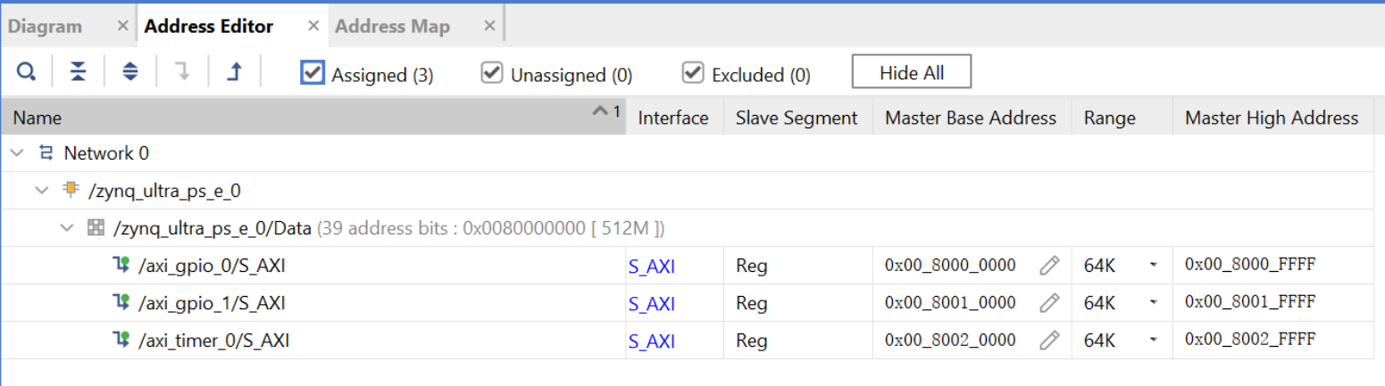
Note: Connection automation assigns addresses automatically. If you connect IP manually, you also need to assign its address.
Exporting the Post-Implementation Hardware Platform
We will run implementation of the Vivado design and export the post-implementation design. The Vivado generated bitstream will be included in the XSA file. It can make the software tests and boot image generation steps easier in the Vitis IDE. Note that the Vitis IDE also accepts pre-synthesis XSAs for application development. Bitstream is only required for debugging PL designs.
Validate the block diagram design:
Return to the block diagram view.
Save the block design (press Ctrl+S).
Click the Validate Design button on the block diagram toolbar. Alternatively, press the F6 key.
It takes a while to validate the design. A message dialog box pops up and states “Validation successful. There are no errors or critical warnings in this design.” If it reports any errors or critical warnings, review the previous steps and correct the errors.
Click OK to close the message.
Generate output products:
Click Generate Block Design in the Flow Navigator panel.
Click Generate,
When the Generate Output Products process completes, click OK.
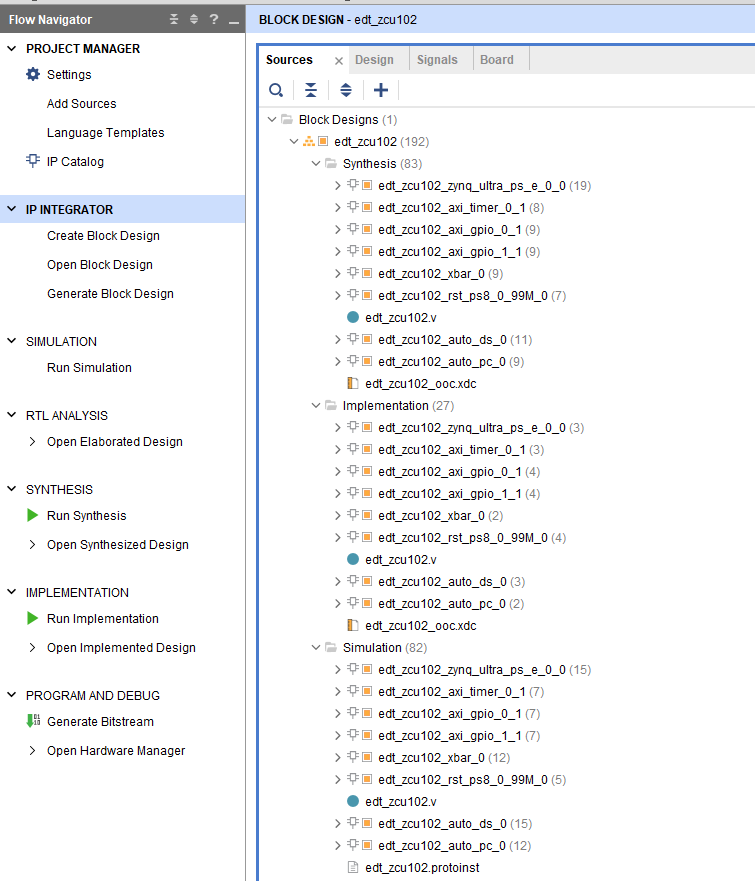
In the Block Diagram Sources window, click the IP Sources tab. Here you can see the output products that you just generated, as shown in the following figure.
Make sure you have an HDL top file. Because this design is saved from the introduction design, we have already done it.
Run synthesis, implementation, and bitstream generation:
Click Generate Bitstream.
Vivado displays a popup message saying “There are no implementation results available. OK to launch synthesis and implementation?”. Click Yes.
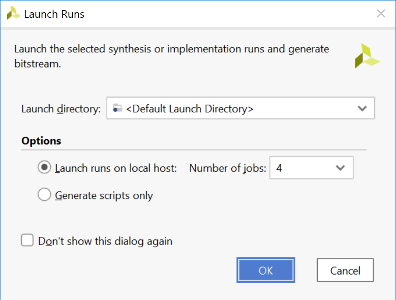
Review the Launch Runs dialogue, set the proper number of jobs to run simultaneously, and click OK.
Wait for Vivado to complete implementation. After it finishes, a Bitstream Generation Completed message will pop up. Click Cancel to close it.
Export the hardware design:
Select File → Export → Export Hardware. The Export Hardware Platform window opens.
Click Next.
Select Include Bitstream and click Next.
Specify the XSA file name and path. This is kept at default in this example. Click Next.
Review the summary and click Finish to close the window.
The hardware platform XSA file is generated in the specified path.
Configuring Software
This use case has a bare-metal application running on an R5 core and a Linux application running on an APU Linux target. Most of the software blocks will remain the same as mentioned in Build Software for PS Subsystems. The software for this design example requires additional drivers for components added in the PL. For this reason, you will need to generate a new bare-metal BSP in the Vitis IDE using the hardware files generated for this design. Linux also requires the Linux BSP to be reconfigured in sync with the new hardware platform file (XSA).
| Processor | Domain | Application |
|---|---|---|
| Cortex-A53 | Linux | ps_pl_linux_app |
| Cortex-R5_0 | Standalone | tmr_psled_r5 |
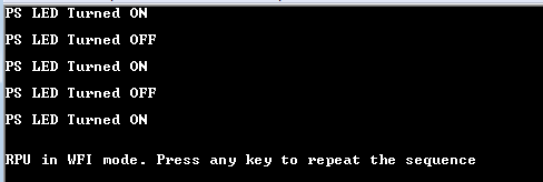
Before you configure the software, first look at the application design scheme. The system has a bare-metal application on RPU, which starts with toggling the PS LEDs for a configurable period. The LEDs are set to toggle in synchronization with a PL AXI Timer running in the PL block. The application sets the AXI Timer in the generate mode and generates an interrupt every time the Timer count expires. The application is designed to toggle the PS LED state after handling the Timer interrupt. The application runs in an infinite while loop and sets the RPU in WFI mode after toggling the LEDs for the configured time period. This LED toggling sequence can be repeated again by getting the RPU out of WFI mode using an external interrupt. For this reason, the UART interrupt is also configured and enabled in the same application. While this application runs on the RPU, the Linux target also hosts another Linux application. The Linux application uses user input from the PS or PL switches to toggle PL LEDs. This Linux application also runs in an infinite while loop, waiting for user input to toggle the PL LEDs. The next set of steps shows how to configure system software and build user applications for this design.
Configuring and Building Linux Using PetaLinux
Create the Linux images using PetaLinux. The Linux images must be created in sync with the hardware configuration for this design. You will also need to configure PetaLinux to create images for SD boot.
Repeat steps 2 to 4 as described in Creating a PetaLinux Image to update the device tree and build Linux images using PetaLinux.
Follow instructions in Verifying the Image on the ZCU102 Board to verify the images.
Make sure you have the following files for creating the Linux domain:
- fsbl.elf
- pmufw.elf
- bl31.elf
- rootfs.ext4
- Image
- system.dtb
Creating the Bare-Metal Application Project
Launch Vitis and use a new workspace C:\edt\design_example_1 for this project.
In the Vitis IDE, select File → New → Application Project. The New Project wizard opens.
Use the information in the table below to make your selections in the wizard.
| Screen | System Properties | Settings |
|---|---|---|
| Platform | Create a New Platform from Hardware | edt_zcu102_wrapper.xsa |
| Generate Boot Components | uncheck | |
| Application Project Details | Application project name | tmr_psled_r5 |
| System project name | tmr_psled_r5_system | |
| Target processor | psu_cortexr5_0 | |
| Domain | Domain | psu_cortexr5_0 |
| Templates | Available templates | Empty Application(C) |
Click Finish.
The New Project wizard closes and the Vitis IDE creates the tmr_psled_r5 application project, which you can view in the Project Explorer.
In the Project Explorer tab, expand the tmr_psled_r5 project.
Right-click the src directory, and select Import to open the Import dialog box.
Expand General in the Import dialog box and select File System.
Click Next.
Select Browse and navigate to the
ref_files/design1folder.Click OK.
Select and add the timer_psled_r5.c file.
Click Finish.
The Vitis IDE automatically builds the application and displays the status in the console window.
Modifying the Linker Script
In the Project Explorer, expand the tmr_psled_r5 project.
In the
srcdirectory, double-clicklscript.ldto open the linker script for this project.In the linker script in Available Memory Regions, modify the following attributes for psu_r5_ddr_0_MEM_0:
Base Address:
0x70000000Size:0x10000000The following figure shows the linker script modification. The following figure is for representation only. Actual memory regions might vary in case of isolation settings.
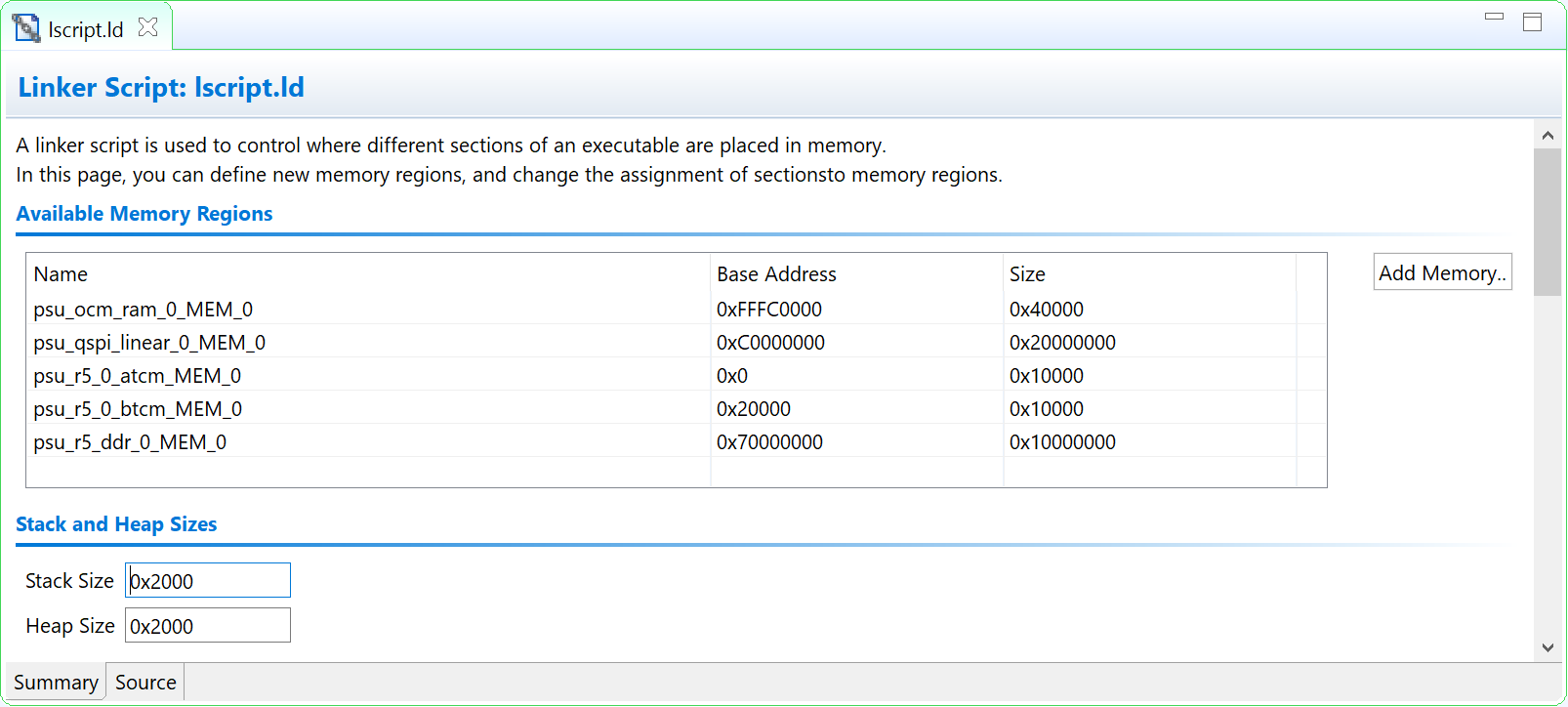
This modification in the linker script ensures that the RPU bare-metal application resides above
0x70000000base address in the DDR, and occupies no more than 256 MB of size.Type Ctrl+S to save the changes.
Modify the BSP to configure UART with UART_1. For more information, see Modifying the Board Support Package for testapp-r5.
Right-click the tmr_psled_r5 project and select Build Project.
Verify that the application is compiled and linked successfully and that the
tmr_psled_r5.elffile is generated in thetmr_psled_r5\Debugfolder.
Creating the Linux Domain for Linux Applications
To create a Linux domain for generating Linux applications, follow these steps:
In the Explorer view of the Vitis IDE, expand the edt_zcu102_wrapper platform project.
Double-click platform.spr in the Explorer view to open the platform explorer.
Click
 in the top right hand corner to add the domain.
When the new domain window opens, enter the following details:
Name: Linux_Domain
Display name: Linux_Domain
OS: Linux
Processor: psu_cortexa53
Supported runtimes: C/C++
Architecture: 64-bit
Bif file: Provide a sample bif file.
Boot Component Directory: Create a boot directory and provide the path.
Linux Image Directory: Provide the same boot directory path.
Build the platform to make the domain change take effects.
Creating the Linux Application Project
In the Vitis IDE, select File → New → Application Project. The New Project wizard opens.
Use the information in the table below to make your selections in the wizard.
| Screen | System Properties | Settings |
|---|---|---|
| Platform | Select platform from repository | edt_zcu102_wrapper |
| Application project details | Application project name | ps_pl_linux_app |
| System project name | ps_pl_linux_app_system | |
| Target processor | psu_cortexa53 SMP | |
| Domain | Domain | Linux_Domain |
| Templates | Available templates | Linux Empty Application |
Since we have already created the Linux domain on psu_cortexa53, it shows up in the target processor list. If you'd like to create the domain during application creation process, you need to check "Show all processors in the hardware specification" to let the wizard show all processors. By default, it only shows the processors that have been used by the domains in the platform.
Click Finish.
The New Project wizard closes and the Vitis IDE creates the ps_pl_linux_app application project, which can be found in the Project Explorer view.
In the Project Explorer view, expand the ps_pl_linux_app project.
Right-click the
srcdirectory, and select Import to open the Import view.Expand General in the Import dialog box and select File System.
Click Next.
Select Browse and navigate to the ref_files/design1 folder.
Click OK.
Select and add the ps_pl_linux_app.c file.
Note: The application might fail to build because of a missing reference to the pthread library. The next section shows how to add the pthread library.
Modifying the Build Settings
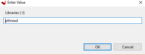
This application makes use of pthreads from the pthread library. Add the pthread library as follows:
Right-click ps_pl_linux_app, and click C/C++ Build Settings.
Refer to the following figures to add the pthread library.
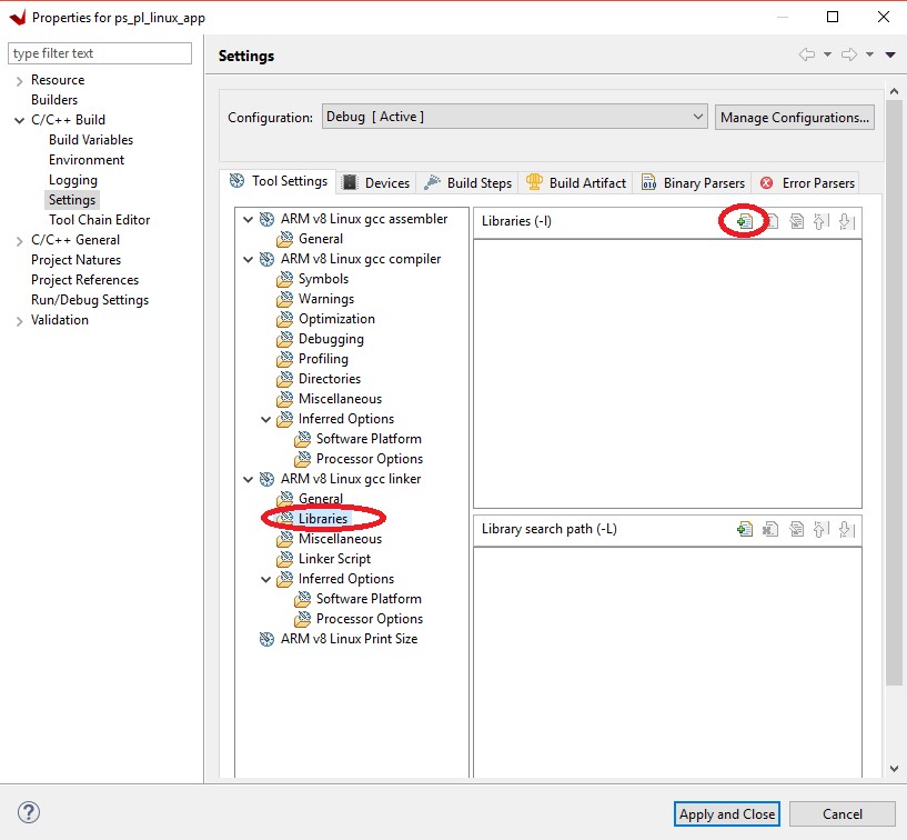
Click OK in both the windows.
Right-click the application and select Build to build the application.
Creating a Boot Image
Now that all the individual images are ready, you will create the boot
image to load all of these components on a Zynq UltraScale+ device. This can be done using the Create Boot Image wizard in the Vitis IDE by performing the following steps. This example creates a boot image BOOT.bin in C:\\edt\\design1.
Launch the Vitis IDE, if it is not already running.
Set the workspace based on the project you created in Zynq UltraScale+ MPSoC Processing System Configuration. For example:
C:\edt.Select Xilinx → Create Boot Image.
In the Create Boot Image wizard, add the settings and partitions as shown in the following figure.
Note: For detailed steps on how to add partitions, see Boot Sequence for SD-Boot.
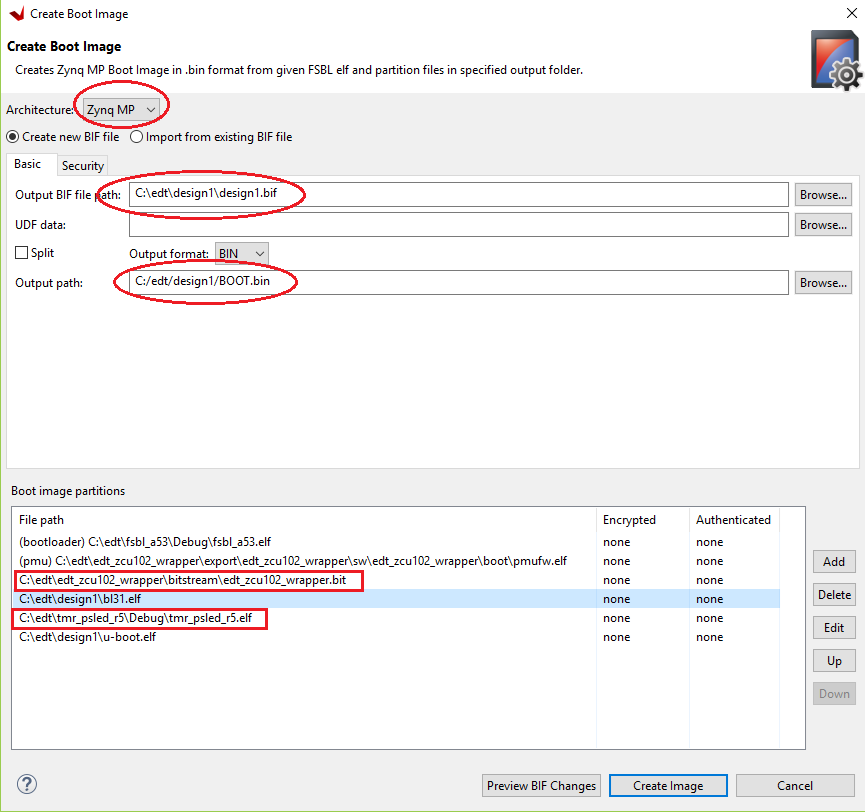
Note: This boot image requires PL bitstream
edt_zcu102_wrapper.bit(Partition Type - Datafile, Destination Device - PL). The bitstream partition needs to be added right after the bootloader while you create the boot image. The R5 applicationtmr_psled_r5.elfis added as partition in this boot image.After adding all the partitions, click Create Image.
IMPORTANT!: Ensure that you have set the correct exception levels for ATF (EL-3, TrustZone) and U-Boot (EL-2) partitions. These settings can be ignored for other partitions.
Running the Image on a ZCU102 Board
Preparing the SD Card
Copy the images and executables onto an SD card and load it into the SD card slot in the board.
Copy the
BOOT.binandimage.ubfiles to an SD card.Note:
BOOT.binis located inC:\edt\design1.Copy the Linux application,
ps_pl_linux_app.elf, to the same SD card. The application can be found inC:\edt\ps_pl_linux_app\Debug.
Target Setup
Load the SD card into the ZCU102 board, in the J100 connector.
Connect the USB-UART on the board to the host machine.
Connect the Micro USB cable into the ZCU102 Board Micro USB port J83, and the other end into an open USB port on the host machine.
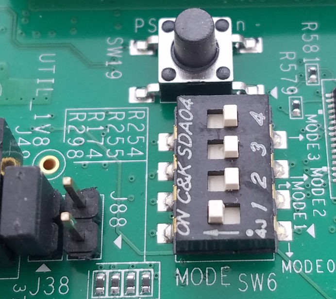
Configure the board to boot in SD boot mode by setting switch SW6 as shown in the following figure.
Connect 12V power to the ZCU102 6-Pin Molex connector.
Start a terminal session, using Tera Term or Minicom depending on the host machine being used, as well as the COM port and baud rate for your system.
For port settings, verify the COM port in the device manager. There are four USB-UART interfaces exposed by the ZCU102 board.
Select the COM port associated with the interface with the lowest number. In this case, for UART-0, select the COM port with interface-0.
Similarly, for UART-1, select the COM port with interface-1. Remember that the R5 BSP has been configured to use UART-1, so R5 application messages will appear on the COM port with the UART-1 terminal.
Power On Target and Run Applications
Turn on the ZCU102 board using SW1, and wait until Linux loads on the board.
You can see the initial boot sequence messages on your terminal screen representing UART-0. The terminal screen configured for UART-1 also prints a message. This is the print message from the R5 bare-metal application running on the RPU, configured to use the UART-1 interface. This application is loaded by the FSBL onto the RPU.
Now that this application is running, notice the PS LED is being toggled by the application, and follow the instructions in the application terminal.
Running Linux Applications
After Linux is up on the ZCU102 system, log into the Linux target with login: root and password: root. The Linux target is now ready to run applications. Run the Linux application by performing the following steps.
Copy the application from the SD card mount point to
/tmp:# cp /run/media/mmcblk0p1/ps_pl_linux_app.elf /tmpNote: Mount the SD card manually if you fail to find SD card contents in this location:
# mount /dev/mmcblk0p1 /media/. Copy the application to/tmp.# cp /media/ps_pl_linux_app.elf /tmp.Run the application.
# /tmp/ps_pl_linux_app.elf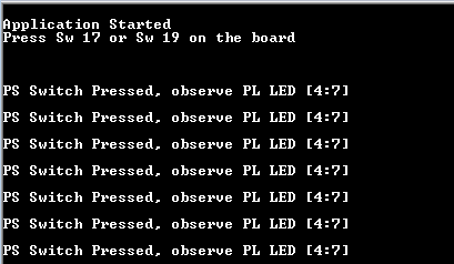
Reference Design Automation
The ref_design for this example provides not only the source code for applications, but also a Makefile to run through the design generation process. To generate the binaries, run the following command:
cd ref_files/design1
make all
Summary
In this design example, you created the hardware design in Vivado with processing system and GPIO modules. The hardware was exported to an XSA file. You imported the hardware to PetaLinux to update the device tree. The regenerated PetaLinux image can boot the board. You also imported the XSA to the Vitis software platform to create the platform project and developed software for Arm Cortex-R5F. You finally created the boot image to include software binaries to run on both the APU and RPU to make the system perform as planned.
The next chapter introduces more boot and configuration techniques.
© Copyright 2017-2021 Xilinx, Inc.
Licensed under the Apache License, Version 2.0 (the “License”); you may not use this file except in compliance with the License. You may obtain a copy of the License at
http://www.apache.org/licenses/LICENSE-2.0
Unless required by applicable law or agreed to in writing, software distributed under the License is distributed on an “AS IS” BASIS, WITHOUT WARRANTIES OR CONDITIONS OF ANY KIND, either express or implied. See the License for the specific language governing permissions and limitations under the License.