2020.1 Vitis™ Application Acceleration Development Flow TutorialsSee 2019.2 Vitis Application Acceleration Development Flow Tutorials |
Data Movement Between the Host and Kernel
In the previous step, you implemented a sequential execution of the written words from the host, computing hash functions on the FPGA, and reading flags by the host.
The compute does not start until the entire input is read into the FPGA, and similarly, the host read from the FPGA does not start until compute is done on the FPGA.
In this lab, you will work with an:
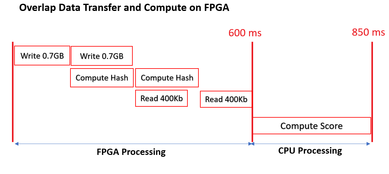
Overlap of host data transfer and compute on the FPGA with split buffers (two buffers)
Split the documents and send them to the FPGA in two iterations.
The kernel can start the compute as soon as the data for the corresponding iteration is transferred to the FPGA.
Overlap of host data transfer and compute with multiple buffers
Explore how the application performance is affected based on splitting the documents and into 2, 4, 8, 16, 32, 64, and 128 chunks.
Overlap data transfer from host, compute on FPGA and profile score on the CPU
Enables the host to start profile scores as soon as the flags are received.
Overlap of Host Data Transfer and Compute with Split Buffers
The following figure illustrates the use case where the input data is split into two sub-buffers.
Host Code Modifications
Navigate to $LAB_WORK_DIR/reference_files, and with a file editor, open run_split_buffer.cpp.
Lines 64 through 148 are modified to optimize the host code to send the input buffer in two iterations which enables the overlap of data transfers with the accelerator execution. The following steps explain the process in detail:
The following two sub-buffers for
input_doc_wordsandoutput_inh_flagsare created.// Make buffers resident in the device q.enqueueMigrateMemObjects({buffer_bloom_filter, buffer_input_doc_words, buffer_output_inh_flags}, CL_MIGRATE_MEM_OBJECT_CONTENT_UNDEFINED); // Specify size of sub-buffers, one for each transaction unsigned subbuf_doc_sz = total_doc_size/2; unsigned subbuf_inh_sz = total_doc_size/2; // Declare sub-buffer regions to specify offset and size of sub-buffer cl_buffer_region subbuf_inh_info[2]; cl_buffer_region subbuf_doc_info[2]; // Declare sub-buffers cl::Buffer subbuf_inh_flags[2]; cl::Buffer subbuf_doc_words[2]; // Specify offset and size of sub-buffers subbuf_inh_info[0]={0, subbuf_inh_sz*sizeof(char)}; subbuf_inh_info[1]={subbuf_inh_sz*sizeof(char), subbuf_inh_sz*sizeof(char)}; subbuf_doc_info[0]={0, subbuf_doc_sz*sizeof(uint)}; subbuf_doc_info[1]={subbuf_doc_sz*sizeof(uint), subbuf_doc_sz*sizeof(uint)}; // Create sub-buffers from buffers based on sub-buffer regions subbuf_inh_flags[0] = buffer_output_inh_flags.createSubBuffer(CL_MEM_WRITE_ONLY, CL_BUFFER_CREATE_TYPE_REGION, &subbuf_inh_info[0]); subbuf_inh_flags[1] = buffer_output_inh_flags.createSubBuffer(CL_MEM_WRITE_ONLY, CL_BUFFER_CREATE_TYPE_REGION, &subbuf_inh_info[1]); subbuf_doc_words[0] = buffer_input_doc_words.createSubBuffer (CL_MEM_READ_ONLY, CL_BUFFER_CREATE_TYPE_REGION, &subbuf_doc_info[0]); subbuf_doc_words[1] = buffer_input_doc_words.createSubBuffer (CL_MEM_READ_ONLY, CL_BUFFER_CREATE_TYPE_REGION, &subbuf_doc_info[1]); printf("\n"); double mbytes_total = (double)(total_doc_size * sizeof(int)) / (double)(1000*1000); double mbytes_block = mbytes_total / 2; printf(" Processing %.3f MBytes of data\n", mbytes_total); printf(" Splitting data in 2 sub-buffers of %.3f MBytes for FPGA processing\n", mbytes_block);
A vector of events are created to coordinate the read, compute, and write operations, so that each iteration is independent of the other iteration, allowing for an overlap between the data transfer and compute.
// Create Events to co-ordinate read,compute and write for each iteration
vector<cl::Event> wordWait;
vector<cl::Event> krnlWait;
vector<cl::Event> flagWait;

printf("--------------------------------------------------------------------\n");

chrono::high_resolution_clock::time_point t1, t2;
t1 = chrono::high_resolution_clock::now();
The kernel arguments are set, and the kernel is enqueued to load the Bloom filter coefficients.
// Only load the Bloom filter in the kernel
cl::Event buffDone,krnlDone,flagDone;
total_size = 0;
load_filter = true;
kernel.setArg(3, total_size);
kernel.setArg(4, load_filter);
q.enqueueMigrateMemObjects({buffer_bloom_filter}, 0, NULL, &buffDone);
wordWait.push_back(buffDone);
q.enqueueTask(kernel, &wordWait, &krnlDone);
krnlWait.push_back(krnlDone);
During the first iteration, the kernel arguments are set, the commands to write the input buffer with first set of words to the FPGA, execute the kernel, and read the results back to the host, are enqueued.
  //  Set Kernel Arguments, Read, Enqueue Kernel and Write for first iteration
  total_size = total_doc_size/2;
  load_filter=false;
  kernel.setArg(3, total_size);
  kernel.setArg(4, load_filter);
  kernel.setArg(0, subbuf_inh_flags[0]);
  kernel.setArg(1, subbuf_doc_words[0]);
  q.enqueueMigrateMemObjects({subbuf_doc_words[0]}, 0, &wordWait, &buffDone);
  wordWait.push_back(buffDone);
  q.enqueueTask(kernel, &wordWait, &krnlDone);
  krnlWait.push_back(krnlDone);
  q.enqueueMigrateMemObjects({subbuf_inh_flags[0]}, CL_MIGRATE_MEM_OBJECT_HOST, &krnlWait, &flagDone);
  flagWait.push_back(flagDone);
During the second iteration, the kernel arguments are set, the commands to write the input buffer with second set of words to the FPGA, execute the kernel, and read the results back to the host, are enqueued.
  //  Set Kernel Arguments, Read, Enqueue Kernel and Write for second iteration
  total_size = total_doc_size/2;
  load_filter=false;
  kernel.setArg(3, total_size);
  kernel.setArg(4, load_filter);
  kernel.setArg(0, subbuf_inh_flags[1]);
  kernel.setArg(1, subbuf_doc_words[1]);
  q.enqueueMigrateMemObjects({subbuf_doc_words[1]}, 0, &wordWait, &buffDone);
  wordWait.push_back(buffDone);
  q.enqueueTask(kernel, &wordWait, &krnlDone);
  krnlWait.push_back(krnlDone);
  q.enqueueMigrateMemObjects({subbuf_inh_flags[1]}, CL_MIGRATE_MEM_OBJECT_HOST, &krnlWait, &flagDone);
  flagWait.push_back(flagDone);
The host waits until the output is read back from the FPGA.
// Wait until all results are copied back to the host before doing the post-processing
 flagWait[0].wait();
 flagWait[1].wait();
Run the Application Using the Bloom8x Kernel
Navigate to the makefile directory, and run the following make command.
cd $LAB_WORK_DIR/makefile; make run STEP=split_buffer TARGET=hw PF=8
The following output displays.
Processing 1398.903 MBytes of data
Split_buffer : Splitting data in 2 sub-buffers of 699.452 MBytes for FPGA processing
--------------------------------------------------------------------
Executed FPGA accelerated version  |   734.0995 ms   ( FPGA 262.363 ms )
Executed Software-Only version     |   3246.2145 ms
--------------------------------------------------------------------
Verification: PASS
Review Profile Report and Timeline Trace for the Bloom8x Kernel
Run the following commands to view the Timeline Trace report with Bloom8x kernel.
vitis_analyzer $LAB_WORK_DIR/build/split_buffer/kernel_8/hw/runOnfpga_hw.xclbin.run_summary
Zoom in to display the following Timeline Trace report.
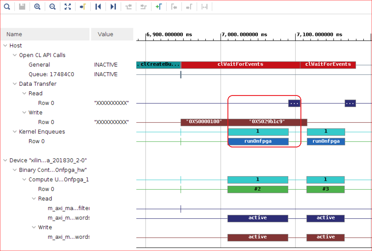
The Timeline Trace confirms that you achieved the execution schedule you expected.
There is an overlap of the read and compute with write operations between the first and second iterations.
The execution time of the first kernel run and the first data read are effectively “hidden” behind the write data transfer from host. This results in a faster overall run.
From the Profile Report, Host Data Transfer: Host Transfer shows that the “data transfer” from the host CPU consumes more than the “Kernel Compute Time”.
The Host to Global Memory WRITE Transfer takes about 178 ms, which is higher compared to using a single buffer.
The Host to Global Memory READ Transfer takes about 38 ms.
Kernels & Compute Unit: Kernel Execution shows that the kernel execution time (calculated by enqueing both compute times) is also higher than when you used a single buffer. When overlapping the host data transfer and kernel, the DDR memory is not exclusive to either the host or kernel which results in a lower performance data transfer. However, you can see that the overall performance is better here compared to the earlier results without splitting words.
When the Bloom8x kernel is used, you can also confirm from the reports that the kernel enqueue time for each compute is smaller than each host transfer. Therefore, there is no real benefit of using the Bloom16x kernel because you are limited by the transfer time from the host. The execution time of the Bloom16x kernel will be faster, but the kernel does not improve the overall application performance. You can confirm this fact by using the Bloom16x kernel in the next step.
Run the Application Using the Bloom16x Kernel
Navigate to the makefile directory, and run the make command.
cd $LAB_WORK_DIR/makefile; make run STEP=split_buffer TARGET=hw PF=16
The following output displays.
Processing 1398.903 MBytes of data
Split_buffer : Splitting data in 2 sub-buffers of 699.452 MBytes for FPGA processing
--------------------------------------------------------------------
Executed FPGA accelerated version  |   733.6324 ms   ( FPGA 233.314 ms )
Executed Software-Only version     |   3133.5186 ms
--------------------------------------------------------------------
Verification: PASS
You can see that if the documents are split into two buffers, the overall application execution time using the Bloom8x kernel and Bloom16x kernel are very close. As expected, using the Bloom16x kernel rather than the Bloom8x kernel has no benefit.
While developing your own application, these attributes can be explored to make trade-offs and pick the optimal kernel implementation optimized for resources/performance.
You will continue this lab with the Bloom8x kernel.
Conclusion
The total execution time on the FPGA has been improved because of the overlapping computation with data transfers. The execution time of the first kernel run and the first data read have been eliminated.
Overlap of Host Data Transfer and Compute with Multiple Buffers
In the previous step, you split the input buffer into two sub-buffers and overlapped the first compute with the second data transfer. In this step, you will write generic code, so the input data is split and processed in an arbitrary number of iterations to achieve the optimal execution time.
Host Code Modifications
Open run_generic_buffer.cpp in $LAB_WORK_DIR/reference_files with a file editor.
Lines 67 through 139 are modified to optimize the host code to send the input buffer in multiple iterations to enable the overlapping of the data transfer and compute. The process is explained in detail as follows:
The following multiple sub-buffers are created for
input_doc_wordsandoutput_inh_flags.// Specify size of sub buffers for each iteration unsigned subbuf_doc_sz = total_doc_size/num_iter; unsigned subbuf_inh_sz = total_doc_size/num_iter; // Declare sub buffer regions to specify offset and size for each iteration cl_buffer_region subbuf_inh_info[num_iter]; cl_buffer_region subbuf_doc_info[num_iter]; // Declare sub buffers cl::Buffer subbuf_inh_flags[num_iter]; cl::Buffer subbuf_doc_words[num_iter]; // Define sub buffers from buffers based on sub-buffer regions for (int i=0; i<num_iter; i++) { subbuf_inh_info[i]={i*subbuf_inh_sz*sizeof(char), subbuf_inh_sz*sizeof(char)}; subbuf_doc_info[i]={i*subbuf_doc_sz*sizeof(uint), subbuf_doc_sz*sizeof(uint)}; subbuf_inh_flags[i] = buffer_output_inh_flags.createSubBuffer(CL_MEM_WRITE_ONLY, CL_BUFFER_CREATE_TYPE_REGION, &subbuf_inh_info[i]); subbuf_doc_words[i] = buffer_input_doc_words.createSubBuffer (CL_MEM_READ_ONLY, CL_BUFFER_CREATE_TYPE_REGION, &subbuf_doc_info[i]); } printf("\n"); double mbytes_total = (double)(total_doc_size * sizeof(int)) / (double)(1000*1000); double mbytes_block = mbytes_total / num_iter; printf(" Processing %.3f MBytes of data\n", mbytes_total); if (num_iter>1) { printf(" Splitting data in %d sub-buffers of %.3f MBytes for FPGA processing\n", num_iter, mbytes_block); }
A vector of events are created to coordinate the read, compute, and write operations, so every iteration is independent of other iterations, which allows for an overlap between the data transfer and compute.
  // Create Events for coordinating read,compute and write for each iteration
    vector<cl::Event> wordWait;
    vector<cl::Event> krnlWait;
    vector<cl::Event> flagWait;

    printf("--------------------------------------------------------------------\n");

    chrono::high_resolution_clock::time_point t1, t2;
    t1 = chrono::high_resolution_clock::now();
The kernel arguments are set, and the kernel is enqueued to load the Bloom filter coefficients.
  // Set Kernel arguments and load the Bloom filter coefficients in the kernel
  cl::Event buffDone, krnlDone;
  total_size = 0;
  load_filter = true;
  kernel.setArg(3, total_size);
  kernel.setArg(4, load_filter);
  q.enqueueMigrateMemObjects({buffer_bloom_filter}, 0, NULL, &buffDone);
  wordWait.push_back(buffDone);
  q.enqueueTask(kernel, &wordWait, &krnlDone);
  krnlWait.push_back(krnlDone);
For each iteration, kernel arguments are set, and the commands to write the input buffer to the FPGA, execute the kernel, and read the results back to the host, are enqueued.
  // Set Kernel arguments. Read, Enqueue Kernel and Write for each iteration
  for (int i=0; i<num_iter; i++)
  {
    cl::Event buffDone, krnlDone, flagDone;
    total_size = subbuf_doc_info[i].size / sizeof(uint);
    load_filter = false;
    kernel.setArg(0, subbuf_inh_flags[i]);
    kernel.setArg(1, subbuf_doc_words[i]);
    kernel.setArg(3, total_size);
    kernel.setArg(4, load_filter);
    q.enqueueMigrateMemObjects({subbuf_doc_words[i]}, 0, &wordWait, &buffDone);
    wordWait.push_back(buffDone);
    q.enqueueTask(kernel, &wordWait, &krnlDone);
    krnlWait.push_back(krnlDone);
    q.enqueueMigrateMemObjects({subbuf_inh_flags[i]}, CL_MIGRATE_MEM_OBJECT_HOST, &krnlWait, &flagDone);
    flagWait.push_back(flagDone);
  }
The host waits until the output of each iteration is read back to the host.
  // Wait until all results are copied back to the host before doing the post-processing
  for (int i=0; i<num_iter; i++)
  {
    flagWait[i].wait();
  }
The code is generic enough to split the data into an arbitrary number of multiple buffers.
Run the Application Using the Bloom8x Kernel
In this step, you will explore the Bloom8x kernel with 100,000 documents split into 2, 4, 8, 16, 32, 64, and 128 chunks, and explore which option results in the best performance.
Go to the
makefiledirectory and run themakecommand.cd $LAB_WORK_DIR/makefile; make run STEP=generic_buffer TARGET=hw PF=8 ITER=8
The argument
ITERcontrols how the input data is split and how many buffers are transferred from the host to the FPGA.Run the same
makecommand with the followingITERvalues: 1, 2, 4, 8, 16, 32, 64.When you run application with multiple
ITERvalues, you will overwrite the output files, such as the Profile Summary report and Timeline Trace. Use the following command to enable the archive_summary feature to save a unique archive file.archive_summary ../build/generic_buffer/kernel_8/hw/runOnfpga_hw.xclbin.run_summary runOnfpga_hw_8.xclbin.run_summary.archive
Use the
vitis_analyzercommand to review and visualize all the reports.bash vitis_analyzer runOnfpga_hw_8.xclbin.run_summary.archive
The following figure shows the plotted graph with the execution times of different
ITERvalues varying withITER.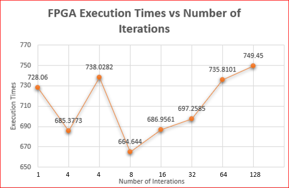
From the graph, you can see that
ITER=8gives the best performance. Your results might differ based on your CPU performance, load on the server, etc.The following output with
ITER8 displays.Processing 1398.907 MBytes of data Generic_Buffer : Splitting data in 8 sub-buffers of 174.863 MBytes for FPGA processing -------------------------------------------------------------------- Executed FPGA accelerated version | 664.6440 ms ( FPGA 224.135 ms ) Executed Software-Only version | 3036.5323 ms -------------------------------------------------------------------- Verification: PASS
Review Profile Report and Timeline Trace for the Bloom8x Kernel
Run the following commands to view the Timeline Trace report with Bloom8x kernel.
vitis_analyzer $LAB_WORK_DIR/build/generic_buffer/kernel_8/hw/runOnfpga_hw.xclbin.run_summary
Zoom in to display the Timeline Trace report.
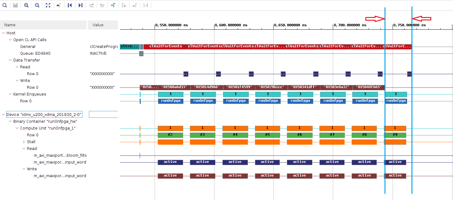
As you can see from the report, the input buffer is split into eight sub buffers, and there are overlaps between read, compute, and write for all iterations. The total computation is divided in eight iterations, but seven of them are occur simultaneously with data transfers; therefore, only the last compute counts towards the total FPGA execution time. This is indicated by the two arrows on timeline trace
You can also see that after splitting the input data into multiple buffers, the total execution time on the FPGA improved from the previous steps, allowing additional overlap between the data transfer and compute.
For your application, the most optimized configuration is:
Bloom8x kernel with the words split in 8 sub-buffers (
ITER=8).
Overlap Between the Host CPU and FPGA
In the previous steps, you looked at optimizing the execution time of the FPGA by overlapping the data transfer from the host to FPGA and compute on the FPGA. After the FPGA compute is complete, the CPU computes the document scores based on the output from the FPGA. Until now, the FPGA processing and CPU post-processing executed sequentially.
If you look at the previous Timeline Trace reports, you can see red segments on the very first row that shows the OpenCL API Calls made by the host application. This indicates that the host is waiting, staying idle while the FPGA computes the hash and flags. In this step, you will overlap the FPGA processing with the CPU post-processing.
Because the total compute is split into multiple iterations, you can start post-processing on the host CPU after the corresponding iteration is complete, allowing the overlap between the CPU and FPGA processing. The performance increases because the CPU is also processing in parallel with the FPGA, which reduces the execution time.
Host Code Modifications
Open
run_sw_overlap.cppin$LAB_WORK_DIR/reference_fileswith a file editor.Lines 134 through 171 are modified to optimize the host code such that CPU processing is overlapped with FPGA processing. It is explained in detail as follows.
The following variables are created to keep track of the words processed by the FPGA.
  // Create variables to keep track of number of words needed by CPU to compute score and number of words processed by FPGA such that CPU processing can overlap with FPGA
  unsigned int curr_entry;
  unsigned char inh_flags;
  unsigned int  available = 0;
  unsigned int  needed = 0;
  unsigned int  iter = 0;
Block the host only if the hash function of the words are still not computed by FPGA, thereby allowing overlap between the CPU and FPGA processing.
  for(unsigned int doc=0, n=0; doc<total_num_docs;doc++)
  {
    unsigned long ans = 0;
    unsigned int size = doc_sizes[doc];

    // Calculate size by needed by CPU for processing next document score
    needed += size;

    // Check if flags processed by FPGA is greater than needed by CPU. Else, block CPU
    // Update the number of available words and sub-buffer count(iter)

    if (needed > available)
    {
      flagWait[iter].wait();
      available += subbuf_doc_info[iter].size / sizeof(uint);
      iter++;
    }

    for (unsigned i = 0; i < size ; i++, n++)
    {
      curr_entry = input_doc_words[n];
      inh_flags  = output_inh_flags[n];

      if (inh_flags)
      {
        unsigned frequency = curr_entry & 0x00ff;
        unsigned word_id = curr_entry >> 8;
        ans += profile_weights[word_id] * (unsigned long)frequency;
      }
    }
    profile_score[doc] = ans;
  }
Run the Application Using the Bloom8x Kernel
Go to the makefile directory, and run the make command.
cd $LAB_WORK_DIR/makefile; make run STEP=sw_overlap TARGET=hw PF=8 ITER=8
The following output displays.
  Processing 1398.905 MBytes of data
  Splitting data in 8 sub-buffers of 174.863 MBytes for FPGA processing
  --------------------------------------------------------------------
  Executed FPGA accelerated version  |   427.1341 ms   ( FPGA 230.345 ms )
  Executed Software-Only version     |   3057.6307 ms
  --------------------------------------------------------------------
  Verification: PASS
Review Profile Report and Timeline Trace for the Bloom8x Kernel
Run the following commands to view the Timeline Trace with Bloom8x kernel.
vitis_analyzer $LAB_WORK_DIR/build/sw_overlap/kernel_8/hw/runOnfpga_hw.xclbin.run_summary
Zoom in to display the Timeline Trace report.
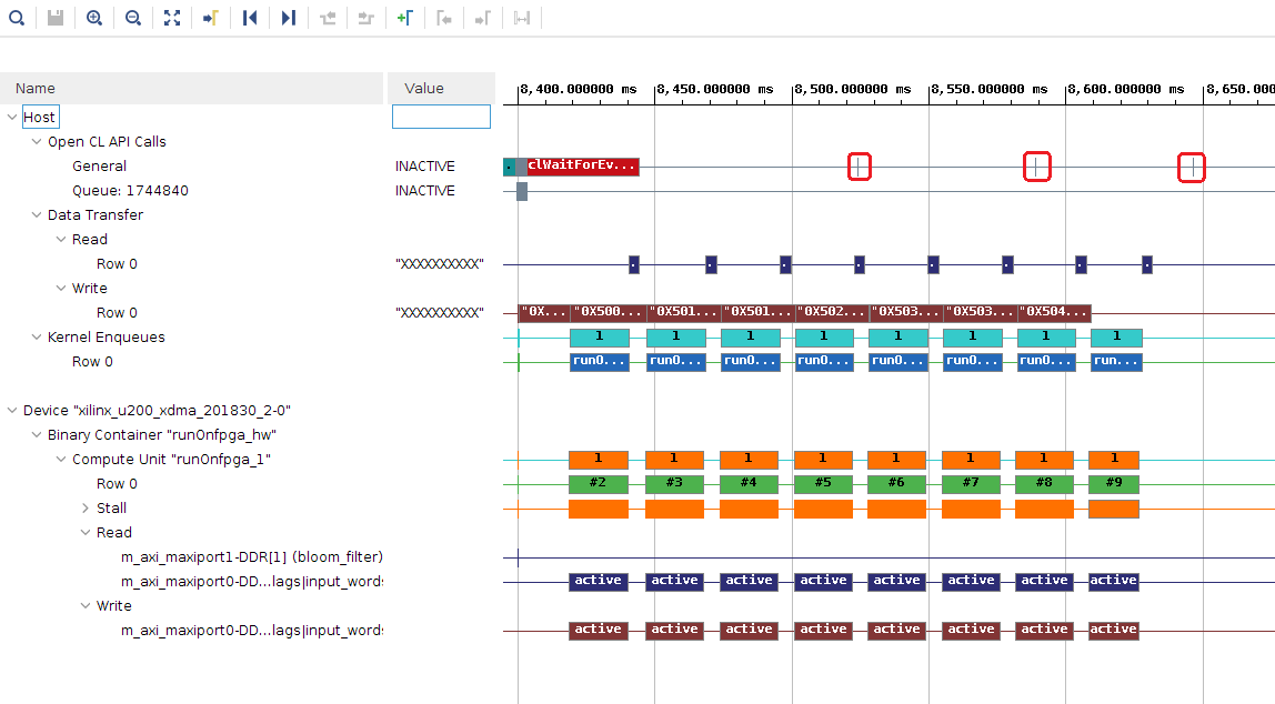
As shown in OpenCL API Calls of the Host section, the red segments are shorter (indicated by red squares) in width which indicates that the processing time of the host CPU is now overlapping with the FPGA processing, which improved the overall application execution time. In the previous steps, the host remained completely idle until the FPGA finished all its processing.
Data Transfer -> Write of the Host section seems to have no gap. Kernel compute time of each invocation is smaller than the Host transfer.
Each Kernel compute and writing flags to DDR are overlapped with the next Host-> Device transfer.
Review Profile Summary Report for the Bloom8x Kernel
Kernels & Compute Unit:Kernel Execution reports 168ms. This should be same as when Bloom8x kernel run with ITER=8.
Kernels & Compute Unit: Compute Unit Stalls section also confirms that “External Memory” stalls are about 20.045 ms compared to no “External Memory” stalls when single buffer was used. This will result in slower data transfer and kernel compute compared to single buffer run.

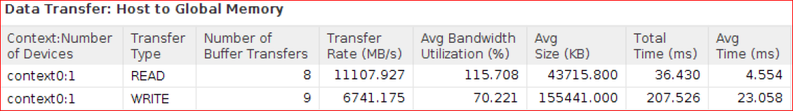
Host Data Transfer: Host Transfer Host to Global Memory WRITE Transfer takes about 207.5 ms and Host to Global Memory READ Transfer takes about 36.4 ms
Kernels & Compute Unit: Compute Unit Utilization section shows that CU Utilization is about 71%. This is an important measure representing how much time CU was active over the Device execution time.

In the next lab, you will compare the results for “Host Data Transfer Rates” and “CU Utilization”.
Throughput Achieved
Based on the results, the throughput of the application is 1399 MB/427 ms = approx 3.27 GBs.` You have now approximately 7.2 times (=3057 ms/427 ms) the performance results compared to the software results.
Opportunities for Performance Improvements
The host and kernel are trying to access the same DDR bank at the same time which resulted in an external memory stall of 20.045 ms. These accesses cause memory contention and limits the speed-up of application execution. In the next module, you will make use of additional bank to minimize the memory contentions.
Return to Getting Started Pathway — Return to Start of Tutorial
Copyright© 2020 Xilinx