 Versal Prime -VMK180 Evaluation Kit PCIe TRD Tutorial |
Hardware Architecture of the Platform |
Hardware Architecture of the Platform
Introduction
This section describes the PCIe platform, in which a media file is transferred from a x86 host machine (root complex) to the VMK180 evaluation board (endpoint) through the PCIe Queue DMA (QDMA).
The design uses the CPM PCI Express (PCIe) Endpoint Hard block in an Gen3 x8 configuration along with QDMA for data transfers between the host system memory and the endpoint.
The QDMA provides protocol conversion between PCIe transaction layer packets (TLPs) and AXI transactions. The DMA cores are used for data transfer between the programmable logic (PL) to the host, and from the host to the PL.
The DMA can transfer data between host and the memory controller (DDR) and from the DDR to the host. The CPM has an AXI Bridge core for AXI-to-host communication. The downstream AXI4-Lite slaves include user-space registers, which are responsible for a hand-shaking mechanism between the host and the endpoint.
Hardware Architecture
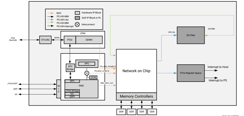
In the host to endpoint direction, the QDMA block moves data from the host memory to the PLside through the PCIe and then writes the data to the memory controller (DDR) via the NOC. Then, the 2D filter accelerator IP reads data from the DDR, performs filtering, and writes it back again to memory. Finally, in the endpoint to host direction, the QDMA reads the DDR via the NOC interface and writes to the host system memory through the PCIe. The following figure shows a detailed hardware block diagram.

Base Platform
The base platform contains the submodules described in this section.
Network On Chip
Versal™ ACAP devices are designed around a network on chip (NoC) interconnect, which provides high-bandwidth communication between different areas of the device. In the base platform, the NoC is used for the following:
Connects the CPM module to DDR memory, allowing the host server to have DMA to the DDR memory controllers.
Allows the Arm®-A72 processor within the processor subsystem (PS) to connect to the DDR memory.
Allows the platform management controller (PMC) to communicate to or from the PCIe and the DDR memory.
Allows all the CPM and PS Cortex-A72 masters to access the programmable logic (PL) peripherals.
Exposes the platform interfaces to connect the accelerator to the base platform, which allows the accelerators to access the DDR memory.
DDR Memory Controllers
The VM1802 device contains four hardened DDR memory controllers (MCs) that are accessed via the NoC. NoC configuration into the MCs can support individual access to each of the four MCs, or alternatively, can support MC interleaving in either pairs or as a group of four. This NoC interleaving ability makes interleaved MCs appear as a single block of memory.
As illustrated in the above figure, the platform design configures all four MCs as a single interleaved bank of memory that in theory can provide up to ~60 Gbytes/second of bandwidth. This memory structure was chosen as a starting point primarily because it is required to support maximum accelerator performance.
CCIX PCIe Module
The CCIX PCIe module (CPM) is the CCIX and the PCIe module, including DMA (QDMA), that is hardened in Versal ACAP devices.
The CPM is configured for Gen3 x8 operation, connecting to the eight adjacent GTY transceivers via the XPIPE dedicated interface as illustrated in the above figure. The PCIe Gen3 x8 transfers data between the accelerator card. The QDMA supports memory mapped AXI operation over the Versal ACAP NoC to allow the host server initiated writes and reads to and from the hardened DDR MCs. This operation is typically known as the QDMA memory mapped operation.
Control Interfaces and Processing System
The control interfaces and processing system (CIPS in the Versal ACAP device contains highperformance Arm Cortex-A72 processors. On-chip and cache memory is included along with a suite of hardened communication peripherals.
A Cortex-A72 device is employed and is given access to 2 GBytes of DDR RAM. This 2 Gbytes of address space is intended solely for the use of the Cortex-A72. Embedded Linux is run on the Cortex-A72, and runs an application to offload the filtering part using XRT by performing scheduling of customer accelerator functions and monitoring for accelerator function completion.
Of the provided PS peripherals, the peripherals required for the accelerator card are as follows:
JTAG/UART: for connection to the Vivado® lab tools (e.g., for bitstream download and debug) and to the on-card satellite controller
I2C: for connection to board peripherals, such as the onboard fan and programmable clock sources
Programmable Logic Infrastructure
The PL logic is shown to stem from the NoC instance as shown in Figure 15. From these NoC connections, the PL peripherals are either directly connected or connected via the intermediate SmartConnect.
User Space Register
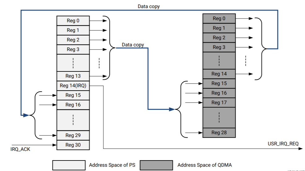
For hand shaking between host and endpoint, the user space register IP is provided. The following figure shows the logical diagram of the IP.
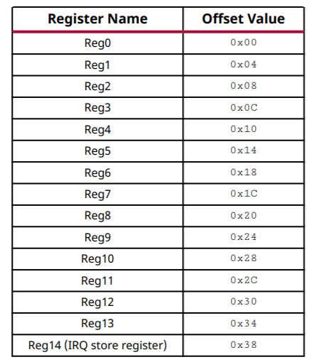
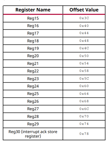
There are 15 32-bit registers starting from offset 0x0000 that have read/write access from the PS. Each register is byte addressable, which means the address for the second register can be calculated by adding four to the address of the first one. Following these are 15 registers that are read-only for the PS and contain values written by the DMA/bridge IP. Reg14 is used as an Interrupt register and reg30 is an Interrupt Acknowledgment register as described in the previous section.
Similarly, there are 15 32-bit registers starting from offset 0x0000 that have read/write access from the host. Following these are 14 registers that are read-only for the host and contain data written by the PS.

Registers available to the PS are listed in the following table. Of these, reg0-reg14 have read and write access and reg15-30 are read-only.
Registers Available to the PS


The same register space is visible to the PCIe DMA with reg0-14 with read/write access and reg15-28 as read-only. Reg29-30 are dummy and are not required.
Next Steps
You can choose any of the following next steps:
Go back to the VMK180 TRD PCIe TRD design start page
License
Licensed under the Apache License, Version 2.0 (the “License”); you may not use this file except in compliance with the License.
You may obtain a copy of the License at http://www.apache.org/licenses/LICENSE-2.0
Unless required by applicable law or agreed to in writing, software distributed under the License is distributed on an “AS IS” BASIS, WITHOUT WARRANTIES OR CONDITIONS OF ANY KIND, either express or implied. See the License for the specific language governing permissions and limitations under the License.
Copyright© 2021 Xilinx