Improving Performance Lab
Introduction
In Introduction to Vitis Part 1 and Part 2, you learned how to create a Vitis project using the GUI and went through the entire design flow. At the end of the lab, you saw the limited transfer bandwidth due to 32-bit data operations. This bandwidth can be improved, and in turn system performance can be improved, by transferring wider data and performing multiple operations in parallel (vectorization). This is one of the common optimization methods to improve kernel performance.
Objectives
After completing this lab, you will learn to:
- Guide the tool to automatically widen the kernel interfaces
- Run Hardware Emulation to see an improvement in bandwidth and runtime
- Perform profile and application timeline analysis in hardware emulation
- Assign AXI4-MM adapters to specific memory banks
Steps
Create a Vitis Project
-
Launch Vitis or continue with your previous session
You can use the same workspace you used in the previous lab
-
Create a new application project and click Next
-
Select
xilinx_aws-vu9p-f1_shell-v04261818_201920_2and click Next -
Name the project wide_vadd and click Next
-
Select
Empty Applicationas the template and click Finish -
Right-click on the wide_vadd_system > wide_vadd > src folder in the Explorer view and select
Import Sources...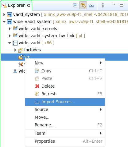
We are going to reuse the host and kernel code from the vadd lab
-
Import all
*.cppand*.hppfiles exceptvadd_krnl.cppfrom~/xup_compute_acceleration/sources/vadd_lab/ -
Similarly, expand wide_vadd_system > wide_vadd_kernels folder in the Explorer view, and import
vadd_krnl.cppin the corresponding src folder -
In the Explorer view, expand the wide_vadd_system > wide_vadd_kernels folder, and double-click on the
wide_vadd_kernels.prj -
Click on
 in the Hardware Functions view and add krnl_vadd function as a Hardware Function (kernel)
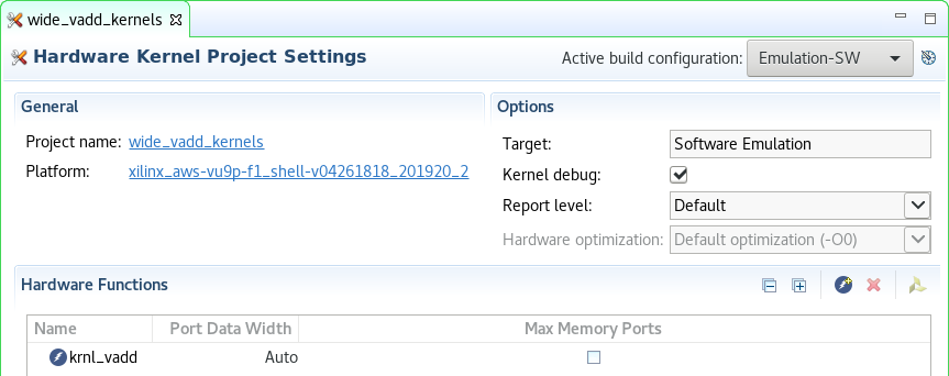
Analyze the kernel code
DDR controllers have a 512-bit wide interface internally. If we parallelize the dataflow in the accelerator, we will be able to read/write 16x 32-bit elements per clock tick instead of one. Thus increasing the effective bandwidth.
-
Double-click on kernel file
krnl_vadd.cppto view its contentLook at lines 40-43 the input vector and output vector are
int(32-bit wide). With small changes in the code and a few directives, we can guide the compiler to widen the the input and output bus to match the memory controller bus, 512-bit wide for this platform.void krnl_vadd(const int* in1, // Read-Only Vector 1 const int* in2, // Read-Only Vector 2 int* out, // Output Result int elements // Number of elements -
The vector add computation is straightforward
for (int i = 0; i < elements; i++) {
   out[i] = in1[i] + in2[i];
}
You will also notice this directive
#pragma HLS LOOP_TRIPCOUNT avg=4096 max=4096 min=4096. As the loop bound is unknown at synthesis, this directive helps the tool to use estimate bounds in the report. This directive has no effect in the synthesized hardware.
Build and run in hardware emulation mode
-
Set Active build configuration: to Emulation-HW
-
Build in Emulation-HW mode by selecting
wide_vadd_systemin the Explorer view and clicking on the build ( ) button
This will take about 10 minutes
-
After build completes, in the Assistant view select wide_vadd_system and click on the Run (
 ) button then select Launch HW Emulator
Analyze the generated design
-
In the Assistant view, double-clicking on
wide_vadd_system > wide_vadd > Emulation-HW > SystemDebugger_wide_vadd_system_wide_vadd > Run Summary (xclbin) -
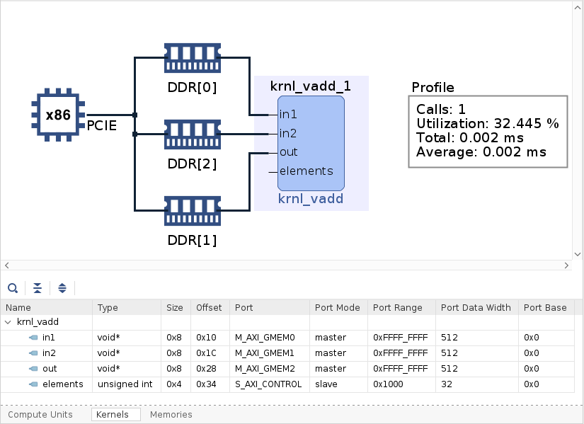
Select System Diagram and click on the Kernels tab on the bottom
Notice that all ports (in1, in2, and out) are using one memory bank. The
Port Data Widthparameter is 32-bit for all arguments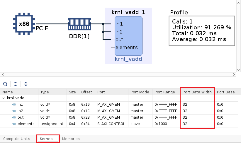
-
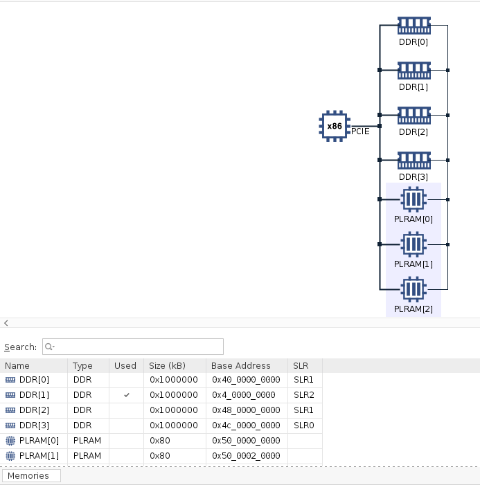
Select Platform Diagram in the left panel
Observe that there are four DDR4 memory banks and three PLRAM banks. In this design,
DDR[1]is used for all operands, which is located in SLR2 (AWS F1)Check memory bank allocation for Alveo U200 and how it relates to AWS-F1 here
-
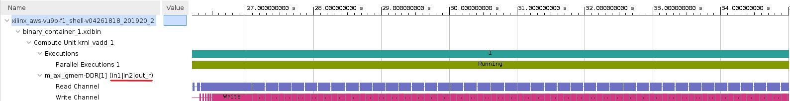
Click on Timeline Trace
-
Scroll and zoom to find the data transfers. The three operands share the same AXI4-MM adapter, both inputs compete in read channel (resource contention). On the other hand, the write channel is independent but it is still mapped to the same memory bank.
-
The Profile Summary reports that the kernel takes 0.035 ms to execute
Operation Naive Kernel Execution - enqueue task 0.035 ms Compute Unit execution time 0.032 ms -
Close Vitis Analyzer
Maximize memory bandwidth and vectorize computation
The host code is executing a 4,096 element vector addition on the vadd kernel. Let us apply optimization techniques to improve the execution time. In this section, we will only consider the latency in clock cycles. Latency in this context means how many cycles it takes for the kernel to be able to process the next 4,096 elements. The 4,096 elements number is only for evaluation purposes and is specified with the LOOP_TRIPCOUNT directive.
-
On the Assistant view, right click on
wide_vadd_system > wide_vadd_kernels > Emulation-HW > krnl_vadd[C/C++]and then click Open HLS Project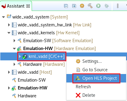
Notice that the Vitis HLS project can only be open once the kernel is synthesized
-
Click
OKwhen prompted to Launch Vitis HLS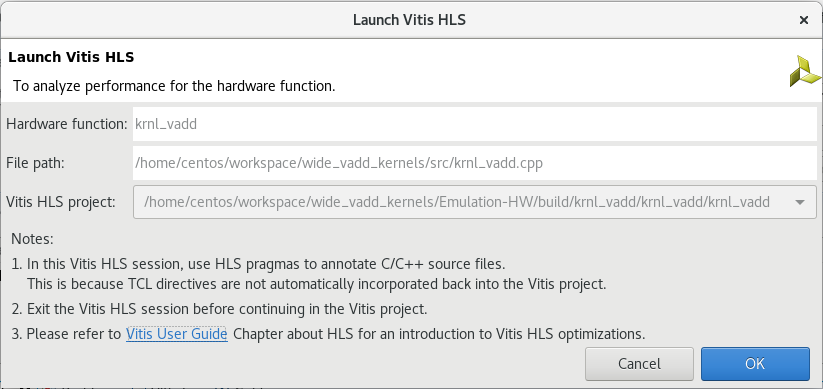
-
In the Synthesis Summary analyze the Performance & Resource Estimates
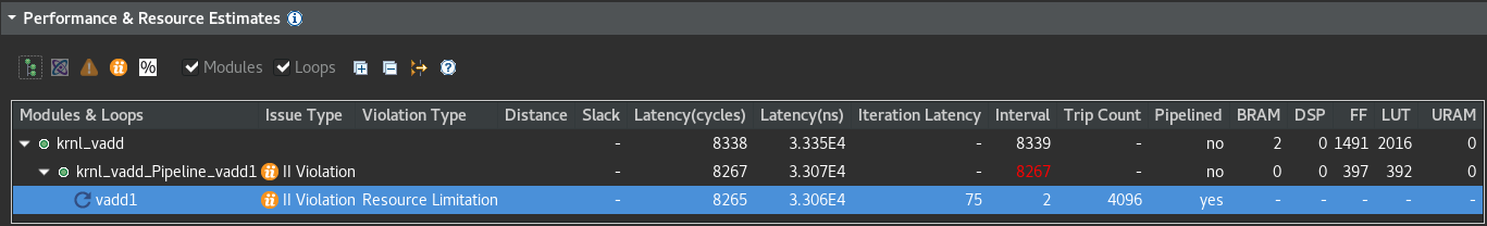
The most internal loop vadd1 has a latency of 8,265 cycles.
Notice that the II violation is because the tool is unable to schedule both read operations on the bus request due to limited memory ports (Resource Limitation).
The suggestion is to consider using a memory core with more ports or partitioning the array.
-
In the Explore view expand Source and double-click on the
krnl_vadd.cppfile to open it
-
In the
krnl_vadd.cppfile, uncomment lines 45, 46 and 47, and save the fileThis will assign one AXI4-MM adapter to each argument
-
Synthesize the kernel by clicking the C synthesis button (
) -
Click OK on the default C Synthesis - Active Solution window
-
In the Synthesis Summary analyze the Performance & Resource Estimates
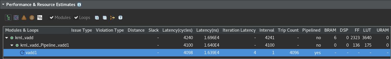
The most internal loop vadd1 has a latency of 4,098 cycles. More than 2x faster by just assigning exclusive resources to each argument.
-
Analyze the HW Interfaces
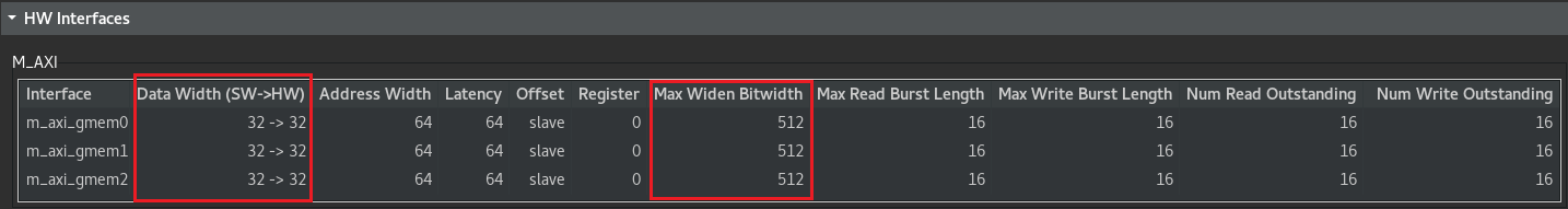
The tool is able to map 32-bit wide operands from software to 32-bit wide operands in hardware. However, we are under utilizing the bus as the memory controller has a 512-bit width bus. Therefore there is an opportunity to fit 16 operands in a 512-bit vector.
-
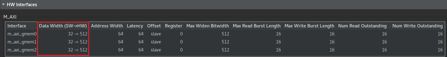
In the
krnl_vadd.cppfile, comment line 51 and uncomment line 52 then save the file and synthesize ()This change in the bounds specifies to the tool that elements is a multiple of 16. Given this guidance the tool is able to fit 16 operands in a 512-bit vector. If the loop bound is known at synthesis and if the operands bitwidth is multiple of it, the compiler will perform this optimization automatically.
Notice that even though we are reading more operands in parallel the latency has not changed.
-
In the
krnl_vadd.cppfile, uncomment line 54 then save the file and synthesize ()The
UNROLLdirective transforms the loop and create N instances of the same operation, thus applying vectorization. In this case, we are unrolling by 16, the same number of operands we can fit in a 512-bit vector. -
In the Synthesis Summary analyze the Performance & Resource Estimates
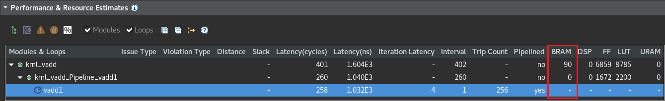
The most internal loop vadd1 has a latency of 258 cycles. Almost 16x faster than without vectorization.
Note that the kernel uses 90 BRAMs, we can reduce this number by mapping two arguments to the same AXI4-MM adapter.
-
In the
krnl_vadd.cppfile modify line 47 to map out tobundle=gmem0and synthesize ()Read and write are independent channels in an AXI4-MM interface, therefore this change will not have an impact on the Latency.
Now the kernel uses 60 BRAMs, 33% less than before.
-
Close Vitis HLS
-
In Vitis, rebuild the project by selecting
wide_vadd_systemin the Explorer view and clicking on the build () button -
After build completes, in the Assistant view select wide_vadd_system and click on the Run (
) button and then select SystemDebugger_wide_vadd_system (System Project Debug) -
In the Assistant view, double-clicking on
wide_vadd_system > wide_vadd > Emulation-HW > SystemDebugger_wide_vadd_system_wide_vadd > Run Summary (xclbin) -
Click on Timeline Trace
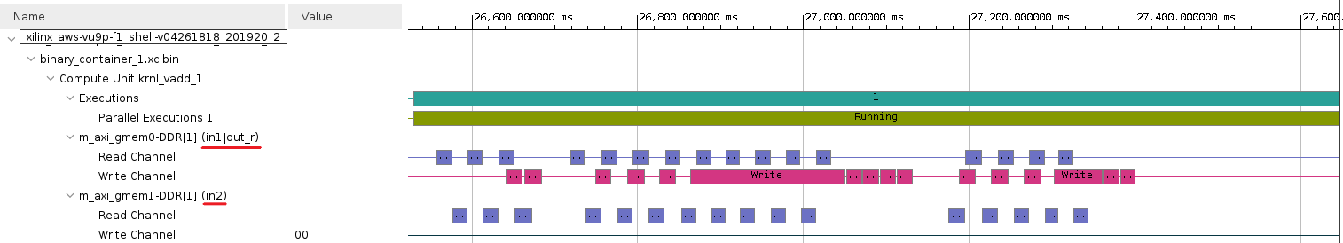
Note that now in1 and in2 are in independent read channels, however access do not overlap. This is due to resource contention as they both access the same memory bank. On the other hand, the write operation overlaps with some of the read operations.
-
Click on Profile Summary and get the Kernel execution time
Operation Naive Optimized Kernel Kernel Execution - enqueue task 0.035 ms 0.006 ms Compute Unit execution time 0.032 ms 0.003 ms
Optimize the system - Use multiple Memory banks
In the previous section, only one memory bank is used. As we have three operands (two read and one write) it may be possible to improve performance by using more memory banks, allowing simultaneous data access and maximizing the bandwidth available for each of the kernel ports. In an AWS-F1 accelerator card, there are four DDR4 memory banks available let us leverage them to reduce resource contention.
To connect a kernel to multiple memory banks, you need to assign each kernel’s port to a memory bank. Note that DDR controllers may be physically located in different SLRs (Super Logic Regions) on the FPGA. A kernel with routing that crosses SLR regions can be more difficult to build and meet timing. This should be taken into account in a real design, where multiple memory banks are located in different SLRs.
-
In the Assistant view, right click on
wide_vadd_system > wide_vadd_system_hw_link > Emulation-HWand then click Settings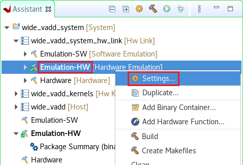
-
In the Binary Container Settings windows, expand
wide_vadd_system_hw_link > Emulation-HWand click binary_container_1 -
Assign the arguments of the
krnl_vaddto the following memory banks- in1 to DDR[0]
- in2 to DDR[2]
- out to DDR[1]
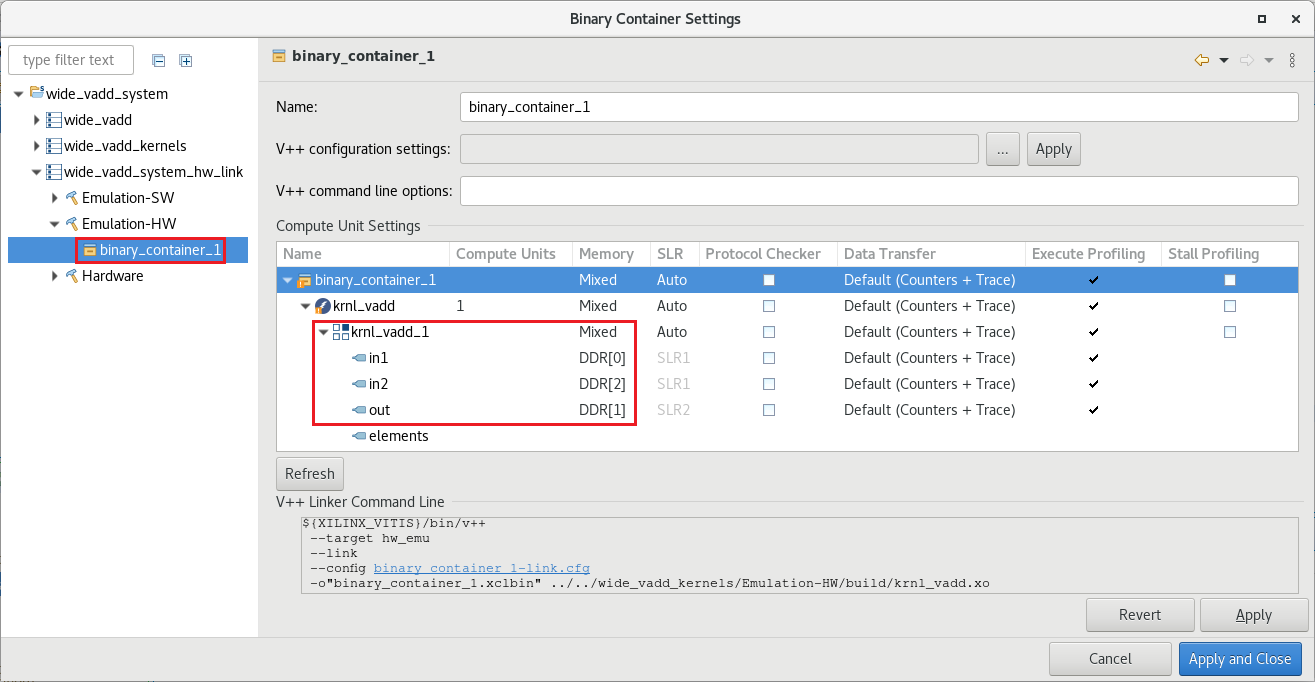
The SLR column is automatically populated after a memory bank is selected
-
Click Apply and Close
-
Rebuild the project by selecting
wide_vadd_systemin the Explorer view and clicking on the build () button -
After build completes, in the Assistant view select wide_vadd_system and click on the Run (
) button and then select SystemDebugger_wide_vadd_system (System Project Debug) -
In the Assistant view, double-clicking on
wide_vadd_system > wide_vadd > Emulation-HW > SystemDebugger_wide_vadd_system_wide_vadd > Run Summary (xclbin) -
Click on Timeline Trace
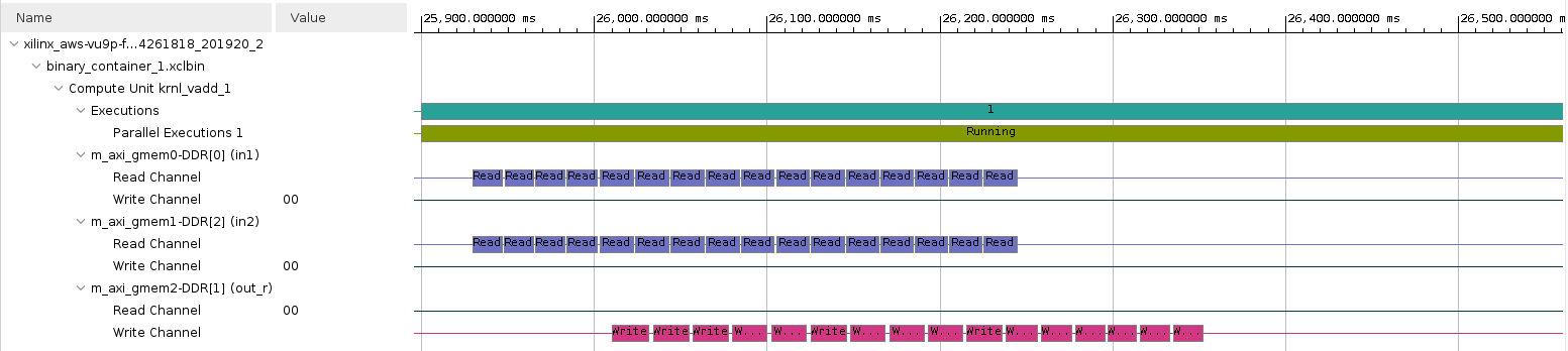
Note that now each argument is mapped to a different memory bank and there is overlap in the read operations.
-
Click on Profile Summary and get the Kernel execution time
Operation Naive Optimized Kernel Optimized Kernel + 3 memory Banks Kernel Execution - enqueue task 0.035 ms 0.006 ms 0.007 ms Compute Unit execution time 0.032 ms 0.003 ms 0.002 ms This time the kernel execution is slighter slower even though the compute unit is faster. This is because the host code is communicating with three different memory banks.
-
Open System Diagram
Notice all ports (in1, in2, and out) are using different memory banks
-
Close Vitis Analyzer
This configuration may be problematic in terms of achieving higher frequency as the kernel is accessing memory banks from different SLRs.
As an exercise for the reader, assign out to DDR[0] (or DDR[2]) and analyze the results. This configuration will utilize memory banks that are in the same SLR. Hint, results below.
| Operation | Naive | Optimized Kernel | Optimized Kernel + 3 memory Banks | Optimized Kernel + 2 memory Banks |
|---|---|---|---|---|
| Kernel Execution - enqueue task | 0.035 ms | 0.006 ms | 0.007 ms | 0.007 ms |
| Compute Unit execution time | 0.032 ms | 0.003 ms | 0.002 ms | 0.002 ms |
Conclusion
From a simple vadd application, we explored steps to optimize kernel and system performance by:
- Using Vitis HLS directives to use multiple AXI4-MM adapters, widen the kernel buses and unrolling the computation loop.
- Assign dedicated memory controller for the arguments
- Use Vitis Analyzer to review the result
The kernel was highly optimized as well as the system. However, the data movement is dominant. To truly achieve acceleration the application has to have a high compute intensity.
The compute intensity ratio is defined as:
compute intensity = compute operations ⁄ memory accesses
The bigger this number is, the more opportunities to achieve acceleration.
Copyright© 2021 Xilinx