AVED - Host to Card Communication
Overview of Physical Function 0
Applications deriving from AVED V80 are inherently PCIe® centric. This section gives an overview of how the AVED hardware design has been configured to facilitate management of the AVED design from the PCIe host via the AMC firmware and companion AVED V80 PCIe driver and utility application.
The Hardware Discovery section explains how the AVED host driver identifies AMD Alveo™ V80 card instances running an application derived from the AVED base design so that the Host OS driver can bind to the card and access the application’s AVED management interface.
The Host to RPU Communication section describes the general principles of message exchange between the host OS and the AMC firmware implementing the AVED management interface for each card instance.
The Host to User Application Communication section suggests ways AVED can be extended to allow application data to be exchanged between application stack running on the PCIe host and the AMD Alveo™ V80 card.
Application developers will naturally alter the AVED base design to optimize application data flow to suit their specific application’s requirements and hence this page offers only high level guidance for user data transport to the Alveo V80 card.
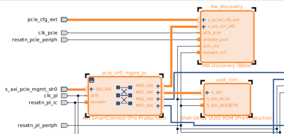
Hardware Discovery
On boot, the host system enumerates the set of PCIe cards in the system and attaches the reference AVED host OS drivers to instances of the Alveo V80 cards it finds running AVED base hardware designs. A full PCIe-based management interface is not available until the AVED host OS driver has attached to the card and acquired a small amount of metadata from the card about its hardware design content. Once the AVED PCIe host driver is attached, the AVED management interface is available to allow the current design content of the AVED V80 cards to be inspected, controlled, and updated.
UUID ROM and PCIe Extended Capabilities
It is helpful to be able to identify which version or build of a design is operating on the FPGA of the Alveo card. In the AVED V80, the base hardware design contains a small AXI peripheral memory that is initialized with a 128-bit UUID value to allow for such design identification. The intent is that the value programmed into the UUID is different for each build of the design. During the AVED build process, the flow scripts compute a hash of the post routed design file and then assign that value into the UUID peripheral’s memory. The AMI driver and command line utility can query for the UUID later when the card is booted and operational in the host system. This allows the driver and the user to identify which iterations of a given AVED base design are operating on each card within the host system.
AVED’s base design includes another piece of IP infrastructure to populate the PCIe extended capabilities configuration space with information about a small number of hardware features in the design. The main purpose of the PCIe extended capabilities content is to inform the AMI software stack of the address offset of a few AXI peripherals (UUID ROM, mailbox, address remapper) within the AVED base hardware design. This information is helpful to know in the earliest stages of the card boot and driver bring-up as it allows early reporting of the UUID ROM content just from the data that can be recovered by system commands, such as lspci. It is worth noting that this convention of address metadata exchange is in place to support successive versioning of a base design over several iterations and design teams. It is possible to simplify the AVED design further by removing the PCIe extended capabilities mechanism provided the address assignments of the AXI peripherals currently presented via in PCIe extended capabilities can be held consistent across design iterations. This tradeoff potentially makes the the software stack more tightly coupled to the addressing conventions of the AVED base design. However, by accepting this tradeoff other design techniques such as PCIe tandem load can be deployed.
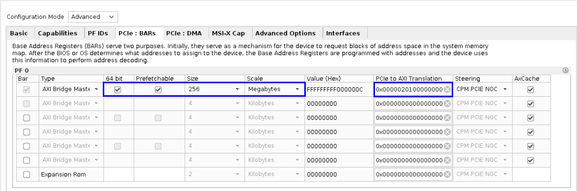
PCIe BAR Layout
The AVED V80 hardware base design declares a single memory aperture for PF0. This memory aperture enables AMI communication to the AMC firmware running on the RPU. Only a subset of this memory will be used in the AVED base design. However, as more features of the processing subsystem are enabled, additional message passing interfaces from the host to, for example, the User OS running in the AMD Versal™ APU, may make use of this memory region.
Host to RPU Communication
The AMI (host OS) and AMC (embedded firmware) components of AVEDs software stack communicate via a region of shared memory and a mailbox peripheral IPs called a generic command queue.
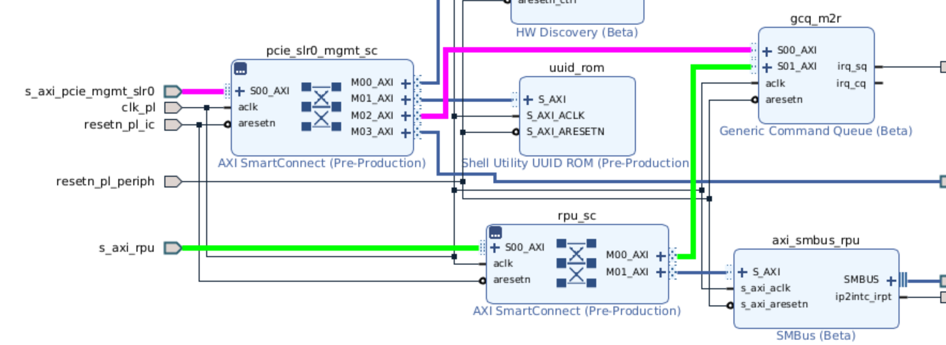
The diagram above shows the PCIe host’s access path to the mailbox (magenta colored nets) and the RPU’s access path to the mailbox (green colored nets). Commands issued to the AVED V80 design via the AMI utility on the PCIe host are transformed into a series of agreed message types that are pushed into the circular buffer of the gcq_m2r IP shown above. The AMC firmware running in the RPU will be alerted to the availability of these messages and (when its control loop allows) begin to service those messages. Internally, the GCQ IP implements a pair of circular buffers to act as submission and completion queues. This allows the RPU to receive commands submitted from the PCIe host and return result codes and other status information on the completion queue. The GCQ IP also implements interrupt services so that software running on the RPU and PCIe host can avoid inefficient polling the card. In the base design, the AMC firmware makes use of interrupts to provide prompt servicing of requests from the AMI software on the host OS. AVED does not have PCIe interrupt architecture requirements to the host OS as it is anticipated that the application interrupt architecture will take precedence over these lower level (and relatively infrequent) command interactions over the management interface.
Host to User Application Communication
Extending the AVED base design to support additional layers of communication, specifically for the user application, will naturally follow the requirements of the specific application being implemented. Some applications may require several PCIe memory apertures to be accessed, others may be satisfied with a very small control interface aperture and data transport via Versal’s PCIe Slave Bridge to the host memory itself. When extending the AVED base design to accommodate application data transport the following extensions to the AVED base design may be common:
Enable additional physical functions to separate application data transport from card management data transport in the Host OS, etc.
Add additional GCQ mailbox IP instances to allow message passing between the user space application on the Host OS and application level firmware operating in the APU.
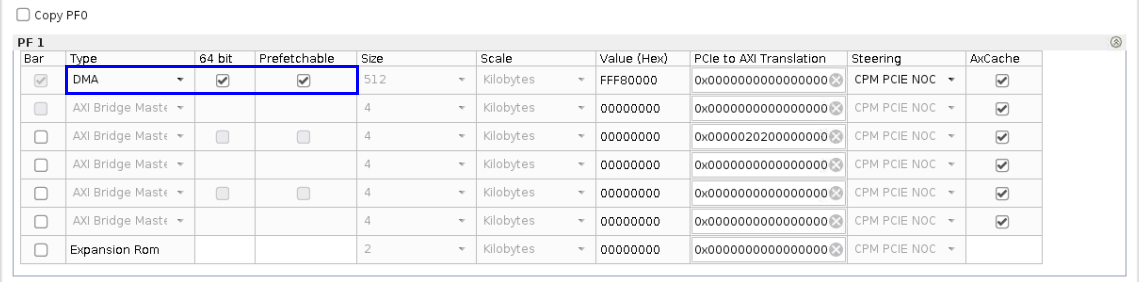
Overview of Physical Function 1
The AVED V80 hardware base design defines PF1 to enable CPM PCIe BAR configurations. This allows DDR and HBM memory to be targeted by CPM DMA transfers to and from host memory.
Page Revision: v. 24