SMBus IP v1.1 - Product Guide
Overview
The SMBus IP provides a mechanism through which a Versal ACAP based system may interact with external devices that are compliant to the System Management Bus (SMBus) v3.2 Specification. SMBus is a two-wire open-drain interface based on the principles of operation defined by the I2C Bus Specification. It provides a standardized control path that enables devices to pass system and power management related messages.
The SMBus IP is designed to be implemented within the PL region of a Versal ACAP and requires connection to I/O Buffers located within an appropriate HDIO bank, these IOBs must be configured to meet the electrical requirements outlined in the SMBus Specification. The IP implements an AXI4-Lite Subordinate memory mapped control interface to enable a processor to interact with other external SMBus devices, the IP supports operation as both a Controller and a multi-device Target to enable multiple management protocols to be implemented simultaneously.
Features
Controller operation
Target operation supporting up to 8 devices
Support for 100KHz, 400KHz or 1MHz operation
Packet Error Correction (PEC) Generation and Checking
Loss of Arbitration detection as a Controller-transmitter
Loss of Arbitration detection as a Target-transmitter
Controller clock synchronization
Controller clock stretching
Target clock stretching
Descriptor based event sequence control
Interrupt driven operation
SMBCLK low timeout detection
SMBDAT low timeout detection
SMBCLK/SMBDAT glitch suppression
SMBCLK stretching timeout detection (Tlow:TEXT/CEXT)
Applications
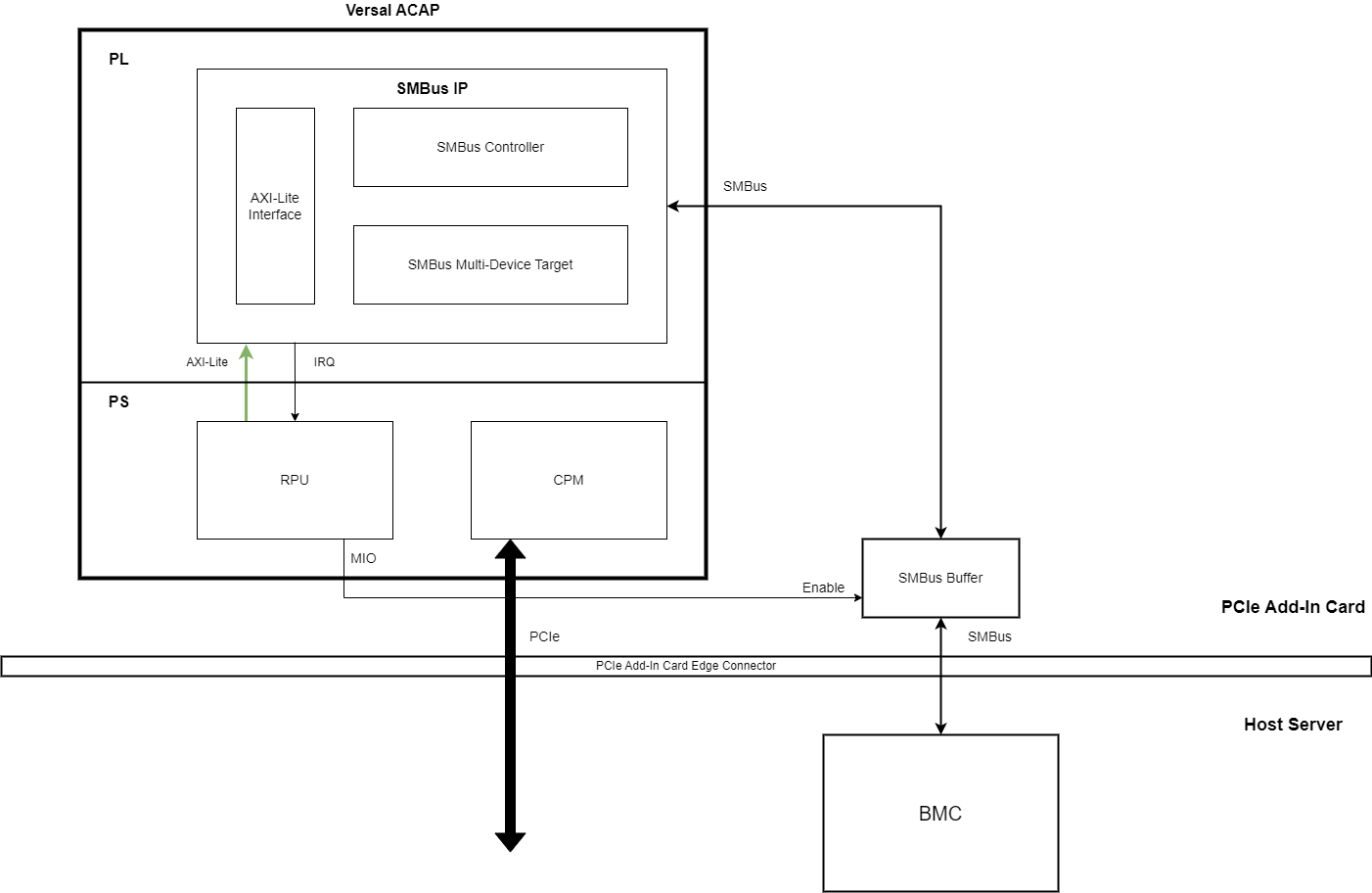
The diagram below outlines a typical use case for the SMBus IP as deployed within a Versal based PCIe add-in accelerator card. The SMBus IP provides a mechanism for the card management software in conjunction with the SMBus IP Driver running on the RPU to communicate with the host server BMC.
Standards
The SMBus IP when implemented in conjunction with the SMBus IP Driver is compliant to the System Management Bus Specification, version 3.2, January 2022 with the following exceptions:
The Quick Command bus protocol is not supported by the SMBus IP for Target device operation.
Architecture Overview
The block diagram below gives a high level overview of the logical structure of the SMBus IP.
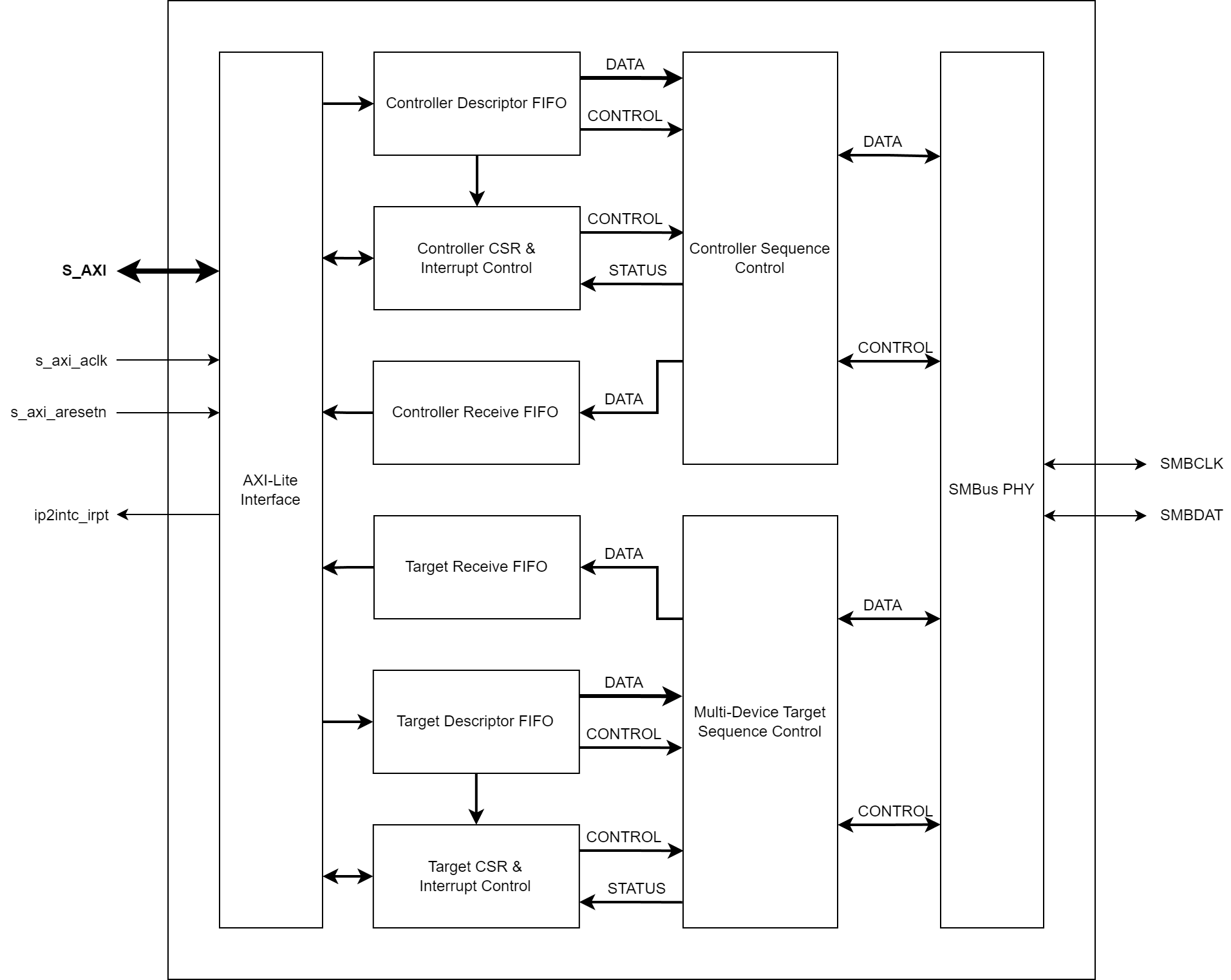
AXI4-Lite Interface
The SMBus IP implements a 32-bit AXI4-Lite Subordinate interface that provides an external processor with memory mapped access to internal register space. The Descriptor/Receive FIFOs and control/status registers that are present within the IP are all accessed via this interface.
Controller Receive FIFO
The Controller Receive FIFO stores bytes that are received by the SMBus IP during Controller Read operations until the processor is ready to read and process theses bytes. The FIFO is arranged as 8-bits x 64 and incorporates a processor programmable fill threshold interrupt that may be configured in order to regulate the rate at which the processor is notified about available data.
Controller Descriptor FIFO
The Controller Descriptor FIFO is used to store the sequence descriptors that are written via the processor interface until they can be executed by the Controller Sequence Control function. Each sequence descriptor instructs the IP to execute a portion of an SMBus packet and may be combined to form any of the Bus Protocols defined in the SMBus Specification.
Controller CSR and Interrupt Control
The Controller Control and Status Registers (CSR) implements the internal control/status registers associated with the Controller Sequence Control function. Relevant semi-static control registers are configured in this function, whereas dynamic control is performed using the sequence descriptors. Interrupt configuration for the interrupt sources generated by the Controller Sequence Control function are also managed within this function.
Controller Sequence Control
The Controller Sequence Control function operates as an SMBus Controller and works in tandem with the SMBus PHY in order to generate the SMBus packet as directed in the received sequence descriptors. The primary functions performed within the Controller Sequence Control function includes:
Reading the Controller Descriptor FIFO and processing the sequence descriptor
Instructing the PHY on when to transmit START/REPEATED-START/STOP conditions on the SMBus
Providing the PHY with transmit bytes during the Controller Write sequences
Reading the assembled received bytes from the PHY during a Controller Read sequence and writing into the Receive FIFO
Performing PEC byte generation and insertion during Controller Write sequences
Performing PEC byte integrity checking on received packets during Controller Read sequences
Status interrupt generation based on events occurring during Read/Write sequences
Target Receive FIFO
The Target Receive FIFO stores bytes that are received by the SMBus IP during Target Write operations until the processor is ready to read and process theses bytes. The FIFO is arranged as 8-bits x 64 and incorporates a processor programmable fill threshold interrupt that may be configured in order to regulate the rate at which the processor is notified about available data.
Target Descriptor FIFO
The Target Descriptor FIFO is used to store the sequence descriptors that are written via the processor interface until they can be executed by the Target Sequence Control function. Each sequence descriptor instructs the IP on how to respond during a Read or Write initiated by an external Controller.
Target CSR and Interrupt Control
The Target Control and Status Registers (CSR) implements the internal control/status registers associated with the Target Sequence Control function. Relevant semi-static control registers are configured in this function, whereas dynamic control is performed using the sequence descriptors. Interrupt configuration for the interrupt sources generated by the Target Sequence Control function are also managed within this function.
Target Sequence Control
The Target Sequence Control function operates as a multi-device SMBus Target that supports operation as up to 8 different devices, each target device address is run time configurable by the processor via the AXI4-Lite interface. The primary functions performed within the Target Sequence Control function includes:
Performing a comparison check on the address received by the PHY following a START condition, against the configured target addresses of interest
Reading the Target Descriptor FIFO and processing the sequence descriptor
Instructing the PHY whether to ACK or NACK a receive byte during a Target Write sequence based on the descriptor
Writing received bytes from the PHY into the Receive FIFO
Providing the PHY with transmit bytes during Target Read sequences based on the payload byte contained in the sequence descriptor
Performing PEC byte integrity checking on received packets during Target Write sequences
Performing PEC byte generation and insertion during Target Read sequences
Status interrupt generation based on events occurring during Read/Write sequences
SMBus PHY
The SMBus PHY provides the physical layer interfacing to the SMBus when connected via Input/Output Buffers in an appropriately configured HDIO bank. The primary functions performed within the SMBus PHY includes:
SMBCLK/SMBDAT input retiming onto the s_axi_aclk domain and noise suppression for glitches <50ns period
SMBCLK/SMBDAT input low timeout and bus idle detection
SMBCLK/SMBDAT output/tri-state control
SMBCLK output low force
Tracking of SMBus state in conjunction with the Target Sequence Control function
Performing SMBCLK clock stretching as a Target when awaiting instruction from the Target Sequence Control function
Transmission of ACK/NACK as a Target-transmitter in accordance with the SMBus AC Specifications
Assembly of receive bytes during Target-receiver operation and forwarding to the Target Sequence Control function for processing
Transmission of read data bytes as a Target-transmitter in accordance with the SMBus AC Specifications
Loss of arbitration detection during Target-transmitter operation
Clock generation and synchronization during Controller operation
START/REPEATED-START/STOP condition transmission as a Controller-transmitter
Transmission of write data bytes as a Controller-transmitter in accordance with the SMBus AC Specifications
Assembly of receive bytes during Controller-receiver operation and forwarding to the Controller Sequence Control function for processing
Loss of arbitration detection during Controller-transmitter operation
Controller Tlow:TEXT timeout detection and Tlow:CEXT measurement
Target Tlow:TEXT measurement
Sequence Descriptors
The SMBus IP is primarily controlled using a set of descriptors, these descriptor sets are independent for both the Target and Controller functions, however the high level behavior is similar. A descriptor consists of a 4-bit ID that instructs the IP on what action to take on the SMBus, along with a payload byte that must be supplied when operating as a transmitter.
Descriptors must be written in the order in which they are to be executed via the AXI4-Lite processor interface to either the Target or Controller Descriptor FIFOs. When the SMBus IP is active for either Target or Controller operation, then it will read and process each descriptor at the appropriate time during either transmission or reception of a SMBus packet. While the IP waits for descriptors, it will perform smbclk clock stretching in order to back-pressure the SMBus until such time that software has determined the next steps and provided the next descriptor.
For scenarios where data on the SMBus must be processed on a byte by byte basis (e.g. Target ARP), then typically only a single descriptor would be supplied at any one time. The IP would execute the descriptor, notify any required response via interrupt, write received data into the Receive FIFO (if applicable) and then begin to clock stretch until software has processed the response and supplied another descriptor.
In other scenarios the sequence of events is known in advance by software, for this the set of descriptors can be written to the Descriptor FIFOs and the IP will process each descriptor without performing any clock stretching. This approach attempts to minimize the amount of software involvement during packet transmission/reception and in turn reduces the amount of clock stretching necessary and the associated risk of exceeding the various clock low extension timeouts outlined in the SMBus Specification e.g. tTIMEOUT, tLOW:TEXT, tLOW:CEXT.
Resource Use
The table below contains resource utilization data for several configurations of the SMBus IP core. Each row within the table describes a test case. The columns are divided into test parameters and results. The test parameters include the part information and the core-specific configuration parameters. Any configuration parameters that are not listed have their default values; any parameters with a blank value are disabled or set automatically by the IP core.
Resource figures are taken from the utilization report issued at the end of implementation using the Out-of-Context flow in Vivado Design Suite.
The Out-of-Context IP constraints include HD.CLK_SRC properties as required to ensure correct hold timing closure: these properties are enabled using the Tcl command: set_param ips.includeClockLocationConstraints true
The frequencies used for clock inputs are stated for each test case.
LUT figures do not include LUTs used as pack-thrus, but do include LUTs used as memory.
Default Vivado Design Suite 2023.1 settings were used. You may be able to improve on these figures using different settings. Because surrounding circuitry will affect placement and timing, no guarantee can be given that these figures will be repeatable in a larger design.
Vivado Release |
Family |
Device |
Package |
Speedgrade |
Configuration Name |
NUM_TARGET_DEVICES |
SMBUS_DEV_CLASS |
FREQ_HZ_AXI_ACLK |
Fixed Clocks |
LUT |
FF |
DSP |
RAMB36 |
RAMB18 |
2023.2 |
versal |
xcv80 |
lsva4737 |
2MHP |
config_0 |
8 |
0 |
95000000 |
s_axi_aclk=95 |
1411 |
1668 |
0 |
0 |
0 |
2023.2 |
versal |
xcv80 |
lsva4737 |
2MHP |
config_1 |
1 |
0 |
95000000 |
s_axi_aclk=95 |
1360 |
1605 |
0 |
0 |
0 |
2023.2 |
versal |
xcv80 |
lsva4737 |
2MHP |
config_2 |
8 |
0 |
500000000 |
s_axi_aclk=500 |
1659 |
1643 |
0 |
0 |
0 |
2023.2 |
versal |
xcv80 |
lsva4737 |
2MHP |
config_3 |
8 |
2 |
500000000 |
s_axi_aclk=500 |
1651 |
1645 |
0 |
0 |
0 |
Interface Descriptions
` </plugins/servlet/confluence/editinword/1118177146/attachments/ipTables.xlsx>`__
Interface |
Signal |
Direction |
Range |
Clock |
Enablement Dependency |
Description |
S_AXI |
s_axi_araddr |
Input |
11:0 |
s_axi_aclk |
TRUE |
AXI4-Lite read address |
S_AXI |
s_axi_arready |
Output |
scalar |
s_axi_aclk |
TRUE |
AXI4-Lite read address ready |
S_AXI |
s_axi_arvalid |
Input |
scalar |
s_axi_aclk |
TRUE |
AXI4-Lite read address valid |
S_AXI |
s_axi_awaddr |
Input |
11:0 |
s_axi_aclk |
TRUE |
AXI4-Lite write address |
S_AXI |
s_axi_awready |
Output |
scalar |
s_axi_aclk |
TRUE |
AXI4-Lite write address ready |
S_AXI |
s_axi_awvalid |
Input |
scalar |
s_axi_aclk |
TRUE |
AXI4-Lite write address valid |
S_AXI |
s_axi_bready |
Input |
scalar |
s_axi_aclk |
TRUE |
AXI4-Lite write response ready |
S_AXI |
s_axi_bresp |
Output |
1:0 |
s_axi_aclk |
TRUE |
AXI4-Lite write response |
S_AXI |
s_axi_bvalid |
Output |
scalar |
s_axi_aclk |
TRUE |
AXI4-Lite write response valid |
S_AXI |
s_axi_rdata |
Output |
31:0 |
s_axi_aclk |
TRUE |
AXI4-Lite read data |
S_AXI |
s_axi_rready |
Input |
scalar |
s_axi_aclk |
TRUE |
AXI4-Lite read ready |
S_AXI |
s_axi_rresp |
Output |
1:0 |
s_axi_aclk |
TRUE |
AXI4-Lite read response |
S_AXI |
s_axi_rvalid |
Output |
scalar |
s_axi_aclk |
TRUE |
AXI4-Lite read valid |
S_AXI |
s_axi_wdata |
Input |
31:0 |
s_axi_aclk |
TRUE |
AXI4-Lite write data |
S_AXI |
s_axi_wready |
Output |
scalar |
s_axi_aclk |
TRUE |
AXI4-Lite write data ready |
S_AXI |
s_axi_wstrb |
Input |
3:0 |
s_axi_aclk |
TRUE |
AXI4-Lite write strobes |
S_AXI |
s_axi_wvalid |
Input |
scalar |
s_axi_aclk |
TRUE |
AXI4-Lite write data valid |
s_axi_aclk |
s_axi_aclk |
Input |
scalar |
TRUE |
Clock associated with the s_axi interface |
|
s_axi_aresetn |
s_axi_aresetn |
Input |
scalar |
s_axi_aclk |
TRUE |
Active-Low reset associated with the s_axi interface |
ip2intc_irpt |
ip2intc_irpt |
Output |
scalar |
s_axi_aclk |
TRUE |
Level High Interrupt |
SMBUS |
smbclk_i |
Input |
scalar |
Asynchronous |
TRUE |
SMBus clock input |
SMBUS |
smbclk_o |
Output |
scalar |
s_axi_aclk |
TRUE |
SMBus clock output |
SMBUS |
smbclk_t |
Output |
scalar |
s_axi_aclk |
TRUE |
SMBus clock output tri-state control |
SMBUS |
smbdat_i |
Input |
scalar |
Asynchronous |
TRUE |
SMBus data input |
SMBUS |
smbdat_o |
Output |
scalar |
s_axi_aclk |
TRUE |
SMBus data output |
SMBUS |
smbdat_t |
Output |
scalar |
s_axi_aclk |
TRUE |
SMBus data output tri-state control |
Clocking
The SMBus IP operates on the s_axi_aclk clock domain, the smbclk_i/smbdat_i asynchronous inputs are retimed onto this clock domain internal to the IP.
The table below outlines the clock frequency ranges supported by the IP.
Clock Domain |
Min (MHz) |
Max (MHz) |
Description |
|---|---|---|---|
s_axi_aclk |
95 |
500 |
Clock used for S_AXI interface and internal core operation. |
Resets
The SMBus IP is reset on assertion of the s_axi_aresetn active low reset input, this input must be synchronous to the s_axi_aclk.
When this reset is asserted, all internal registers are reset to their default values and the Target/Controller logic is brought back to an idle state. Any active SMBus transactions in progress by the IP are aborted.
Interrupts
The SMBus IP operation is interrupt driven so that control information written via the processor interface is sufficiently responsive in order to comply with the timeout limits specified in the SMBus Specification.
Refer to IRQ_IER/IRQ_ISR registers detailed in the Register Space section for information on the SMBus IP interrupt sources.
Register Space
The table below outlines the layout and descriptions for the memory mapped register space within the SMBus IP, these registers are accessible via the AXI4-Lite interface.
Undocumented bits within registers are reserved and are Read-Only.
Register Address Offset |
Register Name |
Field Name |
Bit Index |
Default Value |
Attribute |
Field Description |
|---|---|---|---|---|---|---|
0x000 |
IP_VERSION |
MAJOR_VERSION |
31:16 |
1 |
RO |
IP Major Version
|
MINOR_VERSION |
15:0 |
0 |
RO |
IP Minor Version
|
||
0x004 |
IP_REVISION |
CORE_REVISION |
15:0 |
0 |
RO |
IP Core Revision
|
0x008 |
IP_MAGIC_NUM |
MAGIC_NUMBER |
31:0 |
0x534D_4273 |
RO |
IP Magic Number
|
0x00C |
BUILD_CONFIG_0 |
FREQ_HZ_AXI_ACLK |
31:0 |
* |
RO |
Input AXI ACLK Frequency
|
0x010 |
BUILD_CONFIG_1 |
NUM_TARGET_DEVICES |
7:4 |
* |
RO |
Number of Target Devices supported
|
SMBUS_DEV_CLASS |
1:0 |
* |
RO |
Default SMBus Device Class
|
||
0x020 |
IRQ_GIE |
ENABLE |
0 |
0 |
RW |
Global Interrupt Enable
|
0x024 |
IRQ_IER |
CTLR_DESC_FIFO_ALMOST_EMPTY |
15 |
0 |
RW |
When set, an interrupt will be generated when the IRQ_ISR register reports the CTLR_DESC_FIFO_ALMOST_EMPTY field as set.
|
CTLR_RX_FIFO_FILL_THRESHOLD |
14 |
0 |
RW |
When set, an interrupt will be generated when the IRQ_ISR register reports the CTLR_RX_FIFO_FILL_THRESHOLD field as set.
|
||
CTLR_DESC_FIFO_EMPTY |
13 |
0 |
RW |
When set, an interrupt will be generated when the IRQ_ISR register reports the CTLR_DESC_FIFO_EMPTY field as set.
|
||
CTLR_DONE |
12 |
0 |
RW |
When set, an interrupt will be generated when the IRQ_ISR register reports the CTLR_DONE field as set.
|
||
CTLR_PEC_ERROR |
11 |
0 |
RW |
When set, an interrupt will be generated when the IRQ_ISR register reports the CTLR_PEC_ERROR field as set.
|
||
CTLR_NACK_ERROR |
10 |
0 |
RW |
When set, an interrupt will be generated when the IRQ_ISR register reports the CTLR_NACK_ERROR field as set.
|
||
CTLR_LOA |
9 |
0 |
RW |
When set, an interrupt will be generated when the IRQ_ISR register reports the PHY_CTLR_LOA field as set.
|
||
TGT_DESC_FIFO_ALMOST_EMPTY |
8 |
0 |
RW |
When set, an interrupt will be generated when the IRQ_ISR register reports the TGT_DESC_FIFO_ALMOST_EMPTY field as set.
|
||
TGT_WRITE |
7 |
0 |
RW |
When set, an interrupt will be generated when the IRQ_ISR register reports the TGT_WRITE field as set.
|
||
TGT_READ |
6 |
0 |
RW |
When set, an interrupt will be generated when the IRQ_ISR register reports the TGT_READ field as set.
|
||
TGT_RX_FIFO_FILL_THRESHOLD |
5 |
0 |
RW |
When set, an interrupt will be generated when the IRQ_ISR register reports the TGT_RX_FIFO_FILL_THRESHOLD field as set.
|
||
TGT_DESC_FIFO_EMPTY |
4 |
0 |
RW |
When set, an interrupt will be generated when the IRQ_ISR register reports the TGT_DESC_FIFO_EMPTY field as set.
|
||
TGT_DONE |
3 |
0 |
RW |
When set, an interrupt will be generated when the IRQ_ISR register reports the TGT_DONE field as set.
|
||
TGT_PEC_ERROR |
2 |
0 |
RW |
When set, an interrupt will be generated when the IRQ_ISR register reports the TGT_PEC_ERROR field as set.
|
||
TGT_LOA |
1 |
0 |
RW |
When set, an interrupt will be generated when the IRQ_ISR register reports the TGT_LOA field as set.
|
||
ERROR_IRQ |
0 |
0 |
RW |
When set, an interrupt will be generated when the IRQ_ISR register reports the ERROR_IRQ field as set.
|
||
0x028 |
IRQ_ISR |
CTLR_DESC_FIFO_ALMOST_EMPTY |
15 |
0 |
W1C |
Controller has detected only one descriptor in the Descriptor FIFO and a transaction is in progress
|
CTLR_RX_FIFO_FILL_THRESHOLD |
14 |
0 |
W1C |
Controller Receive FIFO has reached the fill level configured in the CTLR_RX_FIFO_FILL_THRESHOLD register
|
||
CTLR_DESC_FIFO_EMPTY |
13 |
0 |
W1C |
Controller has detected the Descriptor FIFO is empty and another descriptor is required
|
||
CTLR_DONE |
12 |
0 |
W1C |
Controller has successfully completed the transaction
|
||
CTLR_PEC_ERROR |
11 |
0 |
W1C |
Controller has detected a PEC error during a Read transaction with PEC enabled
|
||
CTLR_NACK_ERROR |
10 |
0 |
W1C |
Controller has received a NACK response from the Target following transmission of a byte as Controller-transmitter
|
||
CTLR_LOA |
9 |
0 |
W1C |
Controller has detected loss of arbitration as a Controller-transmitter
|
||
TGT_DESC_FIFO_ALMOST_EMPTY |
8 |
0 |
W1C |
Target has detected only one descriptor in the Descriptor FIFO and a transaction is in progress
|
||
TGT_WRITE |
7 |
0 |
W1C |
Target has detected a start of write transaction for a Target device enabled in TGT_CONTROL_[7:0]
|
||
TGT_READ |
6 |
0 |
W1C |
Target has detected a start of read transaction for a Target device enabled in TGT_CONTROL_[7:0]
|
||
TGT_RX_FIFO_FILL_THRESHOLD |
5 |
0 |
W1C |
Target Receive FIFO has reached the fill level configured in the TGT_RX_FIFO_FILL_THRESHOLD register
|
||
TGT_DESC_FIFO_EMPTY |
4 |
0 |
W1C |
Target has detected the Descriptor FIFO is empty and another descriptor is required
|
||
TGT_DONE |
3 |
0 |
W1C |
Target has detected a STOP condition, transaction is complete and no PEC error detected (if write, if applicable)
|
||
TGT_PEC_ERROR |
2 |
0 |
W1C |
Target has detected a STOP condition, transaction is complete but PEC error detected (only applicable to Writes)
|
||
TGT_LOA |
1 |
0 |
W1C |
Target has detected loss of arbitration as a Target-transmitter
|
||
ERROR_IRQ |
0 |
0 |
W1C |
An error condition has occurred that is both enabled in the ERR_IRQ_IER register and set in the ERR_IRQ_ISR register.
|
||
0x02C |
ERR_IRQ_IER |
PHY_CTLR_CEXT_TIMEOUT |
19 |
0 |
RW |
When set, an error interrupt will be generated when the ERR_IRQ_ISR register reports the PHY_CTLR_CEXT_TIMEOUT field as set.
|
PHY_CTLR_TEXT_TIMEOUT |
18 |
0 |
RW |
When set, an error interrupt will be generated when the ERR_IRQ_ISR register reports the PHY_CTLR_TEXT_TIMEOUT field as set.
|
||
CTLR_RX_FIFO_ERROR |
17 |
0 |
RW |
When set, an error interrupt will be generated when the ERR_IRQ_ISR register reports the CTLR_RX_FIFO_ERROR field as set.
|
||
CTLR_RX_FIFO_OVERFLOW |
16 |
0 |
RW |
When set, an error interrupt will be generated when the ERR_IRQ_ISR register reports the CTLR_RX_FIFO_OVERFLOW field as set.
|
||
CTLR_RX_FIFO_UNDERFLOW |
15 |
0 |
RW |
When set, an error interrupt will be generated when the ERR_IRQ_ISR register reports the CTLR_RX_FIFO_UNDERFLOW field as set.
|
||
CTLR_DESC_FIFO_ERROR |
14 |
0 |
RW |
When set, an error interrupt will be generated when the ERR_IRQ_ISR register reports the CTLR_DESC_FIFO_ERROR field as set.
|
||
CTLR_DESC_FIFO_OVERFLOW |
13 |
0 |
RW |
When set, an error interrupt will be generated when the ERR_IRQ_ISR register reports the CTLR_DESC_FIFO_OVERFLOW field as set.
|
||
CTLR_DESC_FIFO_UNDERFLOW |
12 |
0 |
RW |
When set, an error interrupt will be generated when the ERR_IRQ_ISR register reports the CTLR_DESC_FIFO_UNDERFLOW field as set.
|
||
CTLR_DESC_ERROR |
11 |
0 |
RW |
When set, an error interrupt will be generated when the ERR_IRQ_ISR register reports the CTLR_DESC_ERROR field as set.
|
||
PHY_TGT_TEXT_TIMEOUT |
10 |
0 |
RW |
When set, an error interrupt will be generated when the ERR_IRQ_ISR register reports the PHY_TGT_TEXT_TIMEOUT field as set.
|
||
TGT_RX_FIFO_ERROR |
9 |
0 |
RW |
When set, an error interrupt will be generated when the ERR_IRQ_ISR register reports the TGT_RX_FIFO_ERROR field as set.
|
||
TGT_RX_FIFO_OVERFLOW |
8 |
0 |
RW |
When set, an error interrupt will be generated when the ERR_IRQ_ISR register reports the TGT_RX_FIFO_OVERFLOW field as set.
|
||
TGT_RX_FIFO_UNDERFLOW |
7 |
0 |
RW |
When set, an error interrupt will be generated when the ERR_IRQ_ISR register reports the TGT_RX_FIFO_UNDERFLOW field as set.
|
||
TGT_DESC_FIFO_ERROR |
6 |
0 |
RW |
When set, an error interrupt will be generated when the ERR_IRQ_ISR register reports the TGT_DESC_FIFO_ERROR field as set.
|
||
TGT_DESC_FIFO_OVERFLOW |
5 |
0 |
RW |
When set, an error interrupt will be generated when the ERR_IRQ_ISR register reports the TGT_DESC_FIFO_OVERFLOW field as set.
|
||
TGT_DESC_FIFO_UNDERFLOW |
4 |
0 |
RW |
When set, an error interrupt will be generated when the ERR_IRQ_ISR register reports the TGT_DESC_FIFO_UNDERFLOW field as set.
|
||
TGT_DESC_ERROR |
3 |
0 |
RW |
When set, an error interrupt will be generated when the ERR_IRQ_ISR register reports the TGT_DESC_ERROR field as set.
|
||
PHY_UNEXPTD_BUS_IDLE |
2 |
0 |
RW |
When set, an error interrupt will be generated when the ERR_IRQ_ISR register reports the PHY_UNEXPTD_BUS_IDLE field as set.
|
||
PHY_SMBDAT_LOW_TIMEOUT |
1 |
0 |
RW |
When set, an error interrupt will be generated when the ERR_IRQ_ISR register reports the PHY_SMBDAT_LOW_TIMEOUT field as set.
|
||
PHY_SMBCLK_LOW_TIMEOUT |
0 |
0 |
RW |
When set, an error interrupt will be generated when the ERR_IRQ_ISR register reports the PHY_SMBCLK_LOW_TIMEOUT field as set.
|
||
0x030 |
ERR_IRQ_ISR |
PHY_CTLR_CEXT_TIMEOUT |
19 |
0 |
W1C |
PHY has detected SMBCLK stretching performed by the Controller function beyond the threshold configured in the PHY_CTLR_CEXT_TIMEOUT register
|
PHY_CTLR_TEXT_TIMEOUT |
18 |
0 |
W1C |
Controller has detected SMBCLK stretching performed by an external Target beyond the threshold configured in the PHY_CTLR_TEXT_TIMEOUT register
|
||
CTLR_RX_FIFO_ERROR |
17 |
0 |
W1C |
Controller has detected that an attempt to read or write to the Receive FIFO while it is in reset has been made.
|
||
CTLR_RX_FIFO_OVERFLOW |
16 |
0 |
W1C |
Controller has detected the Receive FIFO has overflowed
|
||
CTLR_RX_FIFO_UNDERFLOW |
15 |
0 |
W1C |
Controller has detected the Receive FIFO has underflowed
|
||
CTLR_DESC_FIFO_ERROR |
14 |
0 |
W1C |
Controller has detected that an attempt to write to the Descriptor FIFO while it is in reset has been made.
|
||
CTLR_DESC_FIFO_OVERFLOW |
13 |
0 |
W1C |
Controller has detected the Descriptor FIFO has overflowed
|
||
CTLR_DESC_FIFO_UNDERFLOW |
12 |
0 |
W1C |
Controller has detected the Descriptor FIFO has underflowed
|
||
CTLR_DESC_ERROR |
11 |
0 |
W1C |
Controller has received an invalid descriptor ID via the Descriptor FIFO or the first descriptor in the sequence is not a START descriptor.
|
||
PHY_TGT_TEXT_TIMEOUT |
10 |
0 |
W1C |
PHY has detected SMBCLK stretching performed by the Target function beyond the threshold configured in the PHY_TGT_TEXT_TIMEOUT register
|
||
TGT_RX_FIFO_ERROR |
9 |
0 |
W1C |
Target has detected that an attempt to read or write to the Receive FIFO while it is in reset has been made.
|
||
TGT_RX_FIFO_OVERFLOW |
8 |
0 |
W1C |
Target has detected the Receive FIFO has overflowed
|
||
TGT_RX_FIFO_UNDERFLOW |
7 |
0 |
W1C |
Target has detected the Receive FIFO has underflowed
|
||
TGT_DESC_FIFO_ERROR |
6 |
0 |
W1C |
Target has detected that an attempt to write to the Descriptor FIFO while it is in reset has been made.
|
||
TGT_DESC_FIFO_OVERFLOW |
5 |
0 |
W1C |
Target has detected the Descriptor FIFO has overflowed
|
||
TGT_DESC_FIFO_UNDERFLOW |
4 |
0 |
W1C |
Target has detected the Descriptor FIFO has underflowed
|
||
TGT_DESC_ERROR |
3 |
0 |
W1C |
Target has received an invalid descriptor via the Descriptor FIFO. This is asserted when either an undefined descriptor ID or unexpected type (e.g. read descriptor during a write) is received.
|
||
PHY_UNEXPTD_BUS_IDLE |
2 |
0 |
W1C |
PHY has detected an unexpected bus idle condition by observing SMBCLK/SMBDAT inputs high beyond the threshold configured in the PHY_IDLE_THRESHOLD register, whilst a transaction is in progress (i.e. no STOP condition)
|
||
PHY_SMBDAT_LOW_TIMEOUT |
1 |
0 |
W1C |
PHY has detected SMBDAT persistently low following a rising edge on SMBCLK for the timeout value configured in the PHY_TIMEOUT_MAX register
|
||
PHY_SMBCLK_LOW_TIMEOUT |
0 |
0 |
W1C |
PHY has detected SMBCLK persistently low for the timeout value configured in the PHY_TIMEOUT_MIN register
|
||
0x034 |
IRQ_ISR_FORCE |
IRQ_ISR_FORCE |
15:0 |
0 |
WO |
Debug IRQ ISR Force
|
0x038 |
ERR_ISR_IRQ_FORCE |
ERR_ISR_IRQ_FORCE |
19:0 |
0 |
WO |
Debug Error IRQ ISR Force
|
0x200 |
PHY_STATUS |
SMBDAT_LOW_TIMEOUT |
2 |
0 |
RO |
Indicates when the SMBus PHY has detected a SMBDAT low timeout in accordance with the threshold configured in the PHY_TIMEOUT_MAX register.
|
SMBCLK_LOW_TIMEOUT |
1 |
0 |
RO |
Indicates when the SMBus PHY has detected a SMBCLK low timeout in accordance with the threshold configured in the PHY_TIMEOUT_MIN register.
|
||
BUS_IDLE |
0 |
0 |
RO |
Indicates when the SMBus PHY has detected the Bus Idle condition
|
||
0x204 |
PHY_FILTER_CONTROL |
ENABLE |
31 |
1 |
RW |
Enable the SMBCLK/SMBDAT input glitch filter
|
DURATION |
4:0 |
* |
RW |
Input Glitch Filter Duration
|
||
0x208 |
PHY_BUS_FREE_TIME |
BUS_FREE_TIME |
11:0 |
* |
RW |
Bus Free Time Control
|
0x20C |
PHY_IDLE_THRESHOLD |
IDLE_THRESHOLD |
14:0 |
* |
RW |
Bus Idle Time Control
|
0x210 |
PHY_TIMEOUT_PRESCALER |
TIMEOUT_PRESCALER |
12:0 |
* |
RW |
Timeout Prescaler Configuration
|
0x214 |
PHY_TIMEOUT_MIN |
TIMEOUT_ENABLE |
31 |
1 |
RW |
Minimum Timeout Detection Enable
|
TIMEOUT_MIN |
11:0 |
* |
RW |
Minimum Timeout Configuration
|
||
0x218 |
PHY_TIMEOUT_MAX |
TIMEOUT_MAX |
11:0 |
* |
RW |
Maximum Timeout Configuration
|
0x21C |
PHY_RESET_CONTROL |
SMBCLK_FORCE_TIMEOUT |
31 |
0 |
WO |
SMBCLK Timeout Force Control
|
SMBCLK_FORCE_LOW |
11:0 |
0 |
RW |
SMBCLK Output Force Control
|
||
0x400 |
PHY_TGT_DATA_SETUP |
TGT_DATA_SETUP |
9:0 |
* |
RW |
Target PHY Data Setup
|
0x404 |
PHY_TGT_TEXT_PRESCALER |
TGT_TEXT_PRESCALER |
8:0 |
* |
RW |
Target PHY TEXT Timeout Prescaler Configuration
|
0x408 |
PHY_TGT_TEXT_TIMEOUT |
TGT_TEXT_TIMEOUT |
14:0 |
* |
RW |
Target PHY TEXT Timeout Configuration
|
0x40C |
PHY_TGT_TEXT_MAX |
TGT_TEXT_MAX |
14:0 |
0 |
WC |
Target PHY TEXT Timeout Max
|
0x410 |
PHY_TGT_DBG_STATE |
DBG_STATE |
7:0 |
0x1 |
RO |
Target PHY Debug State
|
0x414 |
PHY_TGT_DATA_HOLD |
TGT_DATA_HOLD |
9:0 |
* |
RW |
Target PHY Data Hold
|
0x600 |
TGT_STATUS |
ACTIVE |
8 |
0 |
RO |
Indicates that the Target function has received a transaction that matches an enabled address in TGT_CONTROL_[7:0]
|
ADDRESS |
7:1 |
0 |
RO |
Target address for the current transaction, only valid when ACTIVE = 0x1 |
||
RW |
0 |
0 |
RO |
Indicates the current transaction type, only valid when ACTIVE = 0x1
|
||
0x604 |
TGT_DESC_FIFO |
ID |
11:8 |
0 |
WO |
Configure the next Target Descriptor ID
|
PAYLOAD |
7:0 |
0 |
WO |
Configure the next Target Descriptor payload |
||
0x608 |
TGT_DESC_STATUS |
FILL_LEVEL |
14:8 |
0 |
RO |
Indicates the current fill level of the Descriptor FIFO |
FULL |
5 |
0 |
RO |
Indicates if the Descriptor FIFO is full
|
||
ALMOST_FULL |
4 |
0 |
RO |
Indicates if the Descriptor FIFO is almost full
|
||
ALMOST_EMPTY |
1 |
0 |
RO |
Indicates if the Descriptor FIFO is almost empty
|
||
EMPTY |
0 |
0 |
RO |
Indicates if the Descriptor FIFO is empty
|
||
0x60C |
TGT_RX_FIFO |
RESET |
31 |
0 |
WO |
Target Receive FIFO Reset Control
|
PAYLOAD |
7:0 |
0 |
RC |
Receive payload byte for the Target function.
|
||
0x610 |
TGT_RX_FIFO_STATUS |
MAX_FILL_LEVEL |
22:16 |
0 |
W1C |
Indicates the maximum recorded fill level of the Target Receive FIFO |
FILL_LEVEL |
14:8 |
0 |
RO |
Indicates the current fill level of the Target Receive FIFO |
||
RESET_BUSY |
6 |
0 |
RO |
Indicates if the Target Receive FIFO is currently undergoing a reset and is unavailable for either read or write
|
||
FULL |
5 |
0 |
RO |
Indicates if the Target Receive FIFO is full
|
||
ALMOST_FULL |
4 |
0 |
RO |
Indicates if the Target Receive FIFO is almost full
|
||
ALMOST_EMPTY |
1 |
0 |
RO |
Indicates if the Receive FIFO is almost empty
|
||
EMPTY |
0 |
0 |
RO |
Indicates if the Receive FIFO is empty
|
||
0x614 |
TGT_RX_FIFO_FILL_THRESHOLD |
FILL_THRESHOLD |
6:0 |
0x1 |
RW |
Configure the Target Receive FIFO fill threshold that should assert the TGT_RX_FIFO_FILL_THRESHOLD interrupt |
0x618 |
TGT_DBG |
FORCE_PEC_ERROR |
31 |
0x0 |
RW |
Target Debug Force PEC Error
|
DBG_STATE |
6:0 |
0x1 |
RO |
Target Debug State
|
||
0x620 |
TGT_CONTROL_0 |
ENABLE |
31 |
0 |
RW |
Enable for Target Device 0
|
ADDRESS |
7:1 |
0 |
RW |
Address for Target Device 0 |
||
0x624 |
TGT_CONTROL_1 |
ENABLE |
31 |
0 |
RW |
Enable for Target Device 1
|
ADDRESS |
7:1 |
0 |
RW |
Address for Target Device 1 |
||
0x628 |
TGT_CONTROL_2 |
ENABLE |
31 |
0 |
RW |
Enable for Target Device 2
|
ADDRESS |
7:1 |
0 |
RW |
Address for Target Device 2 |
||
0x62C |
TGT_CONTROL_3 |
ENABLE |
31 |
0 |
RW |
Enable for Target Device 3
|
ADDRESS |
7:1 |
0 |
RW |
Address for Target Device 3 |
||
0x630 |
TGT_CONTROL_4 |
ENABLE |
31 |
0 |
RW |
Enable for Target Device 4
|
ADDRESS |
7:1 |
0 |
RW |
Address for Target Device 4 |
||
0x634 |
TGT_CONTROL_5 |
ENABLE |
31 |
0 |
RW |
Enable for Target Device 5
|
ADDRESS |
7:1 |
0 |
RW |
Address for Target Device 5 |
||
0x638 |
TGT_CONTROL_6 |
ENABLE |
31 |
0 |
RW |
Enable for Target Device 6
|
ADDRESS |
7:1 |
0 |
RW |
Address for Target Device 6 |
||
0x63C |
TGT_CONTROL_7 |
ENABLE |
31 |
0 |
RW |
Enable for Target Device 7
|
ADDRESS |
7:1 |
0 |
RW |
Address for Target Device 7 |
||
0x800 |
PHY_CTLR_DATA_HOLD |
CTLR_DATA_HOLD |
14:0 |
* |
RW |
Controller PHY Data Hold
|
0x804 |
PHY_CTLR_START_HOLD |
CTLR_START_HOLD |
14:0 |
* |
RW |
Controller PHY Start Hold
|
0x808 |
PHY_CTLR_START_SETUP |
CTLR_START_SETUP |
14:0 |
* |
RW |
Controller PHY Start Setup
|
0x80C |
PHY_CTLR_STOP_SETUP |
CTLR_STOP_SETUP |
14:0 |
* |
RW |
Controller PHY Stop Setup
|
0x810 |
PHY_CTLR_CLK_TLOW |
CTLR_CLK_TLOW |
14:0 |
* |
RW |
Controller PHY Clock Low
|
0x814 |
PHY_CTLR_CLK_THIGH |
CTLR_CLK_THIGH |
14:0 |
* |
RW |
Controller PHY Clock High
|
0x818 |
PHY_CTLR_TEXT_PRESCALER |
CTLR_TEXT_PRESCALER |
8:0 |
* |
RW |
Controller PHY TEXT Timeout Prescaler Configuration
|
0x81C |
PHY_CTLR_TEXT_TIMEOUT |
CTLR_TEXT_TIMEOUT |
14:0 |
* |
RW |
Controller PHY TEXT Timeout Configuration
|
0x820 |
PHY_CTLR_TEXT_MAX |
CTLR_TEXT_MAX |
14:0 |
* |
WC |
Controller PHY TEXT Timeout Max
|
0x824 |
PHY_CTLR_CEXT_PRESCALER |
CTLR_CEXT_PRESCALER |
8:0 |
* |
RW |
Controller PHY CEXT Timeout Prescaler Configuration
|
0x828 |
PHY_CTLR_CEXT_TIMEOUT |
CTLR_CEXT_TIMEOUT |
13:0 |
* |
RW |
Controller PHY CEXT Timeout Configuration
|
0x82C |
PHY_CTLR_CEXT_MAX |
CTLR_CEXT_MAX |
13:0 |
* |
WC |
Controller PHY CEXT Timeout Max
|
0x830 |
PHY_CTLR_DBG_STATE |
DBG_STATE |
7:0 |
0x1 |
RO |
Controller PHY Debug State
|
0xA00 |
CTLR_CONTROL |
ENABLE |
0 |
0 |
WO |
Controller Enable Control
|
0xA04 |
CTLR_STATUS |
ENABLE |
0 |
0 |
RO |
Controller Enable Status
|
0xA08 |
CTLR_DESC_FIFO |
RESET |
31 |
0 |
WO |
Controller Descriptor FIFO Reset Control
|
ID |
11:8 |
0 |
WO |
Configure the next Controller Descriptor ID
|
||
PAYLOAD |
7:0 |
0 |
WO |
Configure the next Controller Descriptor payload |
||
0xA0C |
CTLR_DESC_STATUS |
FILL_LEVEL |
14:8 |
0 |
RO |
Indicates the current fill level of the Descriptor FIFO |
RESET_BUSY |
6 |
0 |
RO |
Indicates if the Descriptor FIFO is currently undergoing a reset and is unavailable for either read or write
|
||
FULL |
5 |
0 |
RO |
Indicates if the Descriptor FIFO is full
|
||
ALMOST_FULL |
4 |
0 |
RO |
Indicates if the Descriptor FIFO is almost full
|
||
ALMOST_EMPTY |
1 |
0 |
RO |
Indicates if the Descriptor FIFO is almost empty
|
||
EMPTY |
0 |
0 |
RO |
Indicates if the Descriptor FIFO is empty
|
||
0xA10 |
CTLR_RX_FIFO |
RESET |
31 |
0 |
WO |
Controller Receive FIFO Reset Control
|
PAYLOAD |
7:0 |
0 |
RC |
Receive payload byte for the Controller function.
|
||
0xA14 |
CTLR_RX_FIFO_STATUS |
MAX_FILL_LEVEL |
22:16 |
0 |
W1C |
Indicates the maximum recorded fill level of the Controller Receive FIFO |
FILL_LEVEL |
14:8 |
0 |
RO |
Indicates the current fill level of the Controller Receive FIFO |
||
RESET_BUSY |
6 |
0 |
RO |
Indicates if the Controller Receive FIFO is currently undergoing a reset and is unavailable for either read or write
|
||
FULL |
5 |
0 |
RO |
Indicates if the Controller Receive FIFO is full
|
||
ALMOST_FULL |
4 |
0 |
RO |
Indicates if the Controller Receive FIFO is almost full
|
||
ALMOST_EMPTY |
1 |
0 |
RO |
Indicates if the Controller Receive FIFO is almost empty
|
||
EMPTY |
0 |
0 |
RO |
Indicates if the Controller Receive FIFO is empty
|
||
0xA18 |
CTLR_RX_FIFO_FILL_THRESHOLD |
FILL_THRESHOLD |
6:0 |
0x1 |
RW |
Configure the Controller Receive FIFO fill threshold that should assert the CTLR_RX_FIFO_FILL_THRESHOLD interrupt |
0xA1C |
CTLR_DBG |
FORCE_PEC_ERROR |
31 |
0x0 |
RW |
Controller Debug Force PEC Error
|
DBG_STATE |
8:0 |
0x1 |
RO |
Controller Debug State
|
||
Customizing and Generating the IP
This section includes information about using AMD tools to customize and generate the SMBus IP using Vivado Design Suite.
If you are customizing and generating the IP in the Vivado IP integrator, see the Vivado Design Suite User Guide: Designing IP Subsystems using IP Integrator(UG994) for detailed information.
Importing the IP Repository
The SMBus IP is delivered as a standalone IP repository that can be imported for use within Vivado Design Suite. Refer to the Vivado Design Suite User Guide: Designing with IP(UG896) for detailed information on adding an external IP repository to a project.
Customizing the IP
You can customize the IP for use in your design by specifying values for the various User Parameters associated with the IP.
Parameters
The table below details the User Parameters that may be configured for the SMBus IP along with the associated model parameters and default settings.
Display Name |
User Parameter |
Model Parameter |
Model Parameter Format / Range |
Default |
Description |
|---|---|---|---|---|---|
Default SMBus Device Class |
SMBUS_DEV_CLASS |
C_SMBUS_DEV_CLASS |
integer = {0 = 100KHz, 1 = 400KHz, 2 = 1MHz} |
0 |
|
Target Devices |
NUM_TARGET_DEVICES |
C_NUM_TARGET_DEVICES |
integer = {1..8} |
8 |
|
S_AXI Clock Frequency (Hz) |
FREQ_HZ_AXI_ACLK |
C_FREQ_HZ_AXI_ACLK |
integer = {95000000..500000000} |
100000000 |
Configure the input clock frequency of the s_axi_aclk clock in hertz.
|
Output Generation
For detailed information on generating IP output products, please refer to the Vivado Design Suite User Guide: Designing with IP (UG896).
Constraining the IP
The SMBUS interface on the IP includes the necessary I/O buffer controls and is intended to be connected to the design top level ports. When the IP implemented within an IP Integrator block design context, then the generated BD wrapper will automatically include the required IOB components and connectivity from the SMBus IP.
The top level IOB connections must be constrained at the design top level depending upon the IO bank type to which the SMBus IP is connected. The following constraint properties must be considered, however the required settings will be dependent upon the connectivity of the IOBs in the end application:
PACKAGE_PIN
IOSTANDARD
DRIVE
SLEW
Refer to the Vivado Design Suite User Guide: Using Constraints (UG903) for detailed information on defining physical constraints.
Simulation
For comprehensive information about Vivado simulation components, as well as information about using supported third-party tools, see the Vivado Design Suite User Guide: Logic Simulation(UG900).
Synthesis and Implementation
For details about synthesis and implementation, see the Vivado Design Suite User Guide: Designing with IP (UG896).
Driver
The SMBus IP must be used in conjunction with the SMBus IP Driver in order to implement a SMBus v3.2 compliant solution. Please refer to the SMBus IP Driver Specification for detailed information.
Example Design
The SMBus IP does not currently support generation of an IP example design.
Page Revision: v. 5