AVED V80 - Memory Map
AVED uses the address mapping illustrated below.
Memory Mapping
This table shows the recommended functions that can access the DDR Memories. The light grey rows and columns related to the APU, PCIe User, and PCIe DMA are not currently used, but they are captured for future growth. The Yes/No entries indicate the recommended memory access. There is not an active control that prohibits unintended access to the DDR. For example, if caution is not exercised, the APU or PL could access DDR locations intended for the RPU (RPU execution).
Address remapping must be used for the PCIe to access the 128MB of memory starting at 0x000_3800_0000. The address remap is configured in the AXI NoC CIPS (axi_noc_cips).
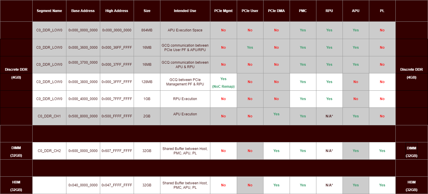
N/A* The RPU is only 32-bit addressing, so it cannot access more than 4GB of DDR.
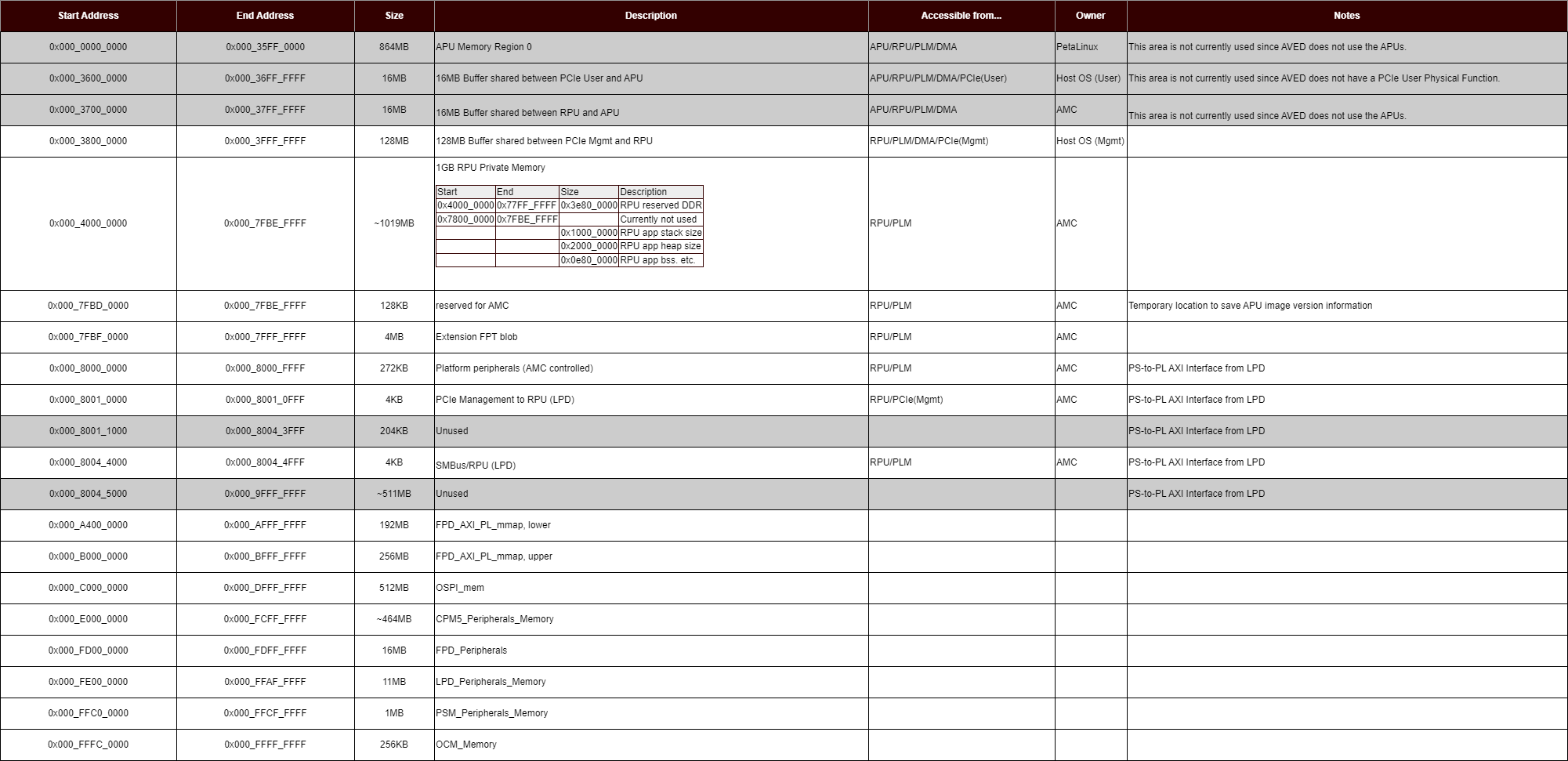
AVED Memory Map
This table shows the memory map of AVED. The greyed out rows are not used in AVED, but they are available for future growth.
A complete AMD Versal™ Address map can be found here:
https://docs.xilinx.com/r/en-US/am011-versal-acap-trm/4-GB-Processor-System-Address-Map
https://docs.xilinx.com/r/en-US/am011-versal-acap-trm/16-TB-Address-Map
AVED 4G Memory Space - DDR Lower 2G & PS/PMC
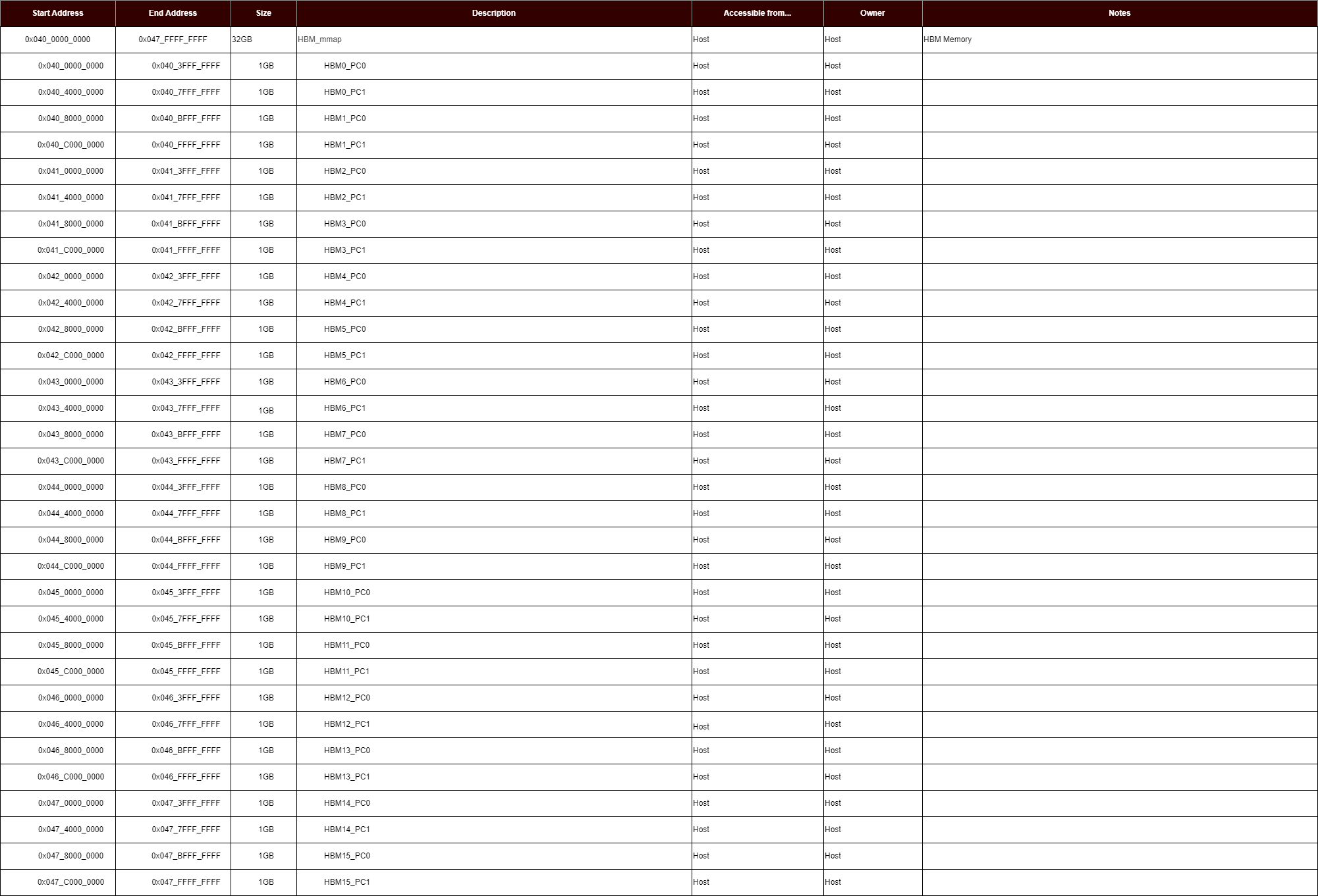
AVED HBM Memory Space
AVED PL Memory Space
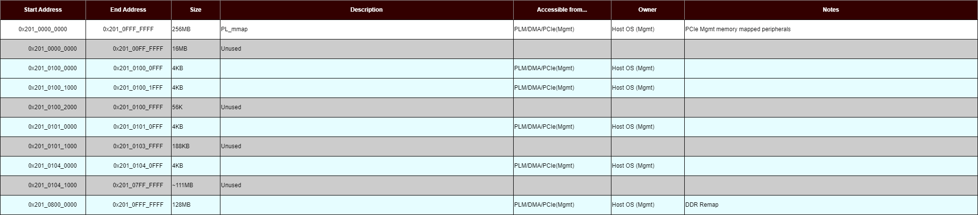
PCIe® Management functions are in blue.
AVED DDR Upper 2G and DIMM 32G Memory Space

Page Revision: v. 81