Using the Zynq SoC Processing System
The Zynq SoC consists of Arm® Cortex™-A9 cores, many hard intellectual property components (IPs), and programmable logic (PL). This offering can be used in two ways:
The Zynq SoC PS can be used in a standalone mode, without attaching any additional fabric IP.
IP cores can be instantiated in fabric and attached to the Zynq PS as a PS+PL combination.
This chapter looks at how to develop an embedded system with only the processing system (PS) of the Zynq®-7000 SoC.
The creation of a Zynq device system design involves configuring the PS to select the appropriate boot devices and peripherals. To start with, as long as the PS peripherals and available MIO connections meet the design requirements, no bitstream is required. This chapter guides you through creating a simple PS-based design that does not require a bitstream.
Example 1 uses Vivado to design the hardware project of this embedded system.
Example 2 designs a “Hello World” software application in the Vitis IDE based on the Example 1 hardware.
Example 1: Creating a New Embedded Project with Zynq SoC
For this example, you will launch the Vivado Design Suite and create a project with an embedded processor system as the top level.
Input and Output Files
Input Files: N/A
Output Files: Vivado hardware handoff file system_wrapper.xsa
Creating Your Hardware Design
Start the Vivado Design Suite.
On Windows 10, click the start menu and find Xilinx Design Tools -> Vivado 2021.2.
On Linux, run source <Vivado installation path>/settings64.sh to set up the environment and run
vivado &to launch the Vivado IDE.
In the Vivado Quick Start page, click Create Project to open the New Project wizard.
Use the information in the table below to make selections in each of the wizard screens.
Screen
System Property
Setting or Command to Use
Project Name
Project name
edt_zc702
Project Location
C:/edt
Create Project Subdirectory
Leave this checked.
Project is an extensible Vitis platform
Leave this unchecked.
Project Type
Specify the type of sources for your design. You can start with RTL or a synthesized EDIF.
RTL Project
Do not specify sources at this time
Leave this checked.
Project is a an extensible Vitis platform
Leave this unchecked.
Default Part
Choose a default Xilinx part or board for your project
Select the Boards tab.
Boards
ZYNQ-7 ZC702 Evaluation Board
New Project roject Summary
Project Summary
Review the project summary.
Click Finish. The New Project wizard closes and the project you just created opens in the Vivado design tool.
Creating an Embedded Processor Block Diagram
Perform the following steps to create an embedded processor project.
Create a new block diagram:
In the Flow Navigator, under IP Integrator, click Create Block Design.
The Create Block Design dialog box opens.
Update Design Name if necessary. In this example, change it to system.
Click OK.
The Diagram window opens with a message that states that this design is empty. To get started, you will next add some IP from the catalog.
Add the Zynq Processing System IP to the block diagram:
Click the Add IP button
 .
.In the search box, type zynq to find the Zynq device IP options.
Double-click the ZYNQ7 Processing System IP to add it to the block design.
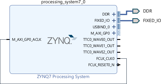
The Zynq Processing System IP block appears in the Diagram view, as shown in the following figure.
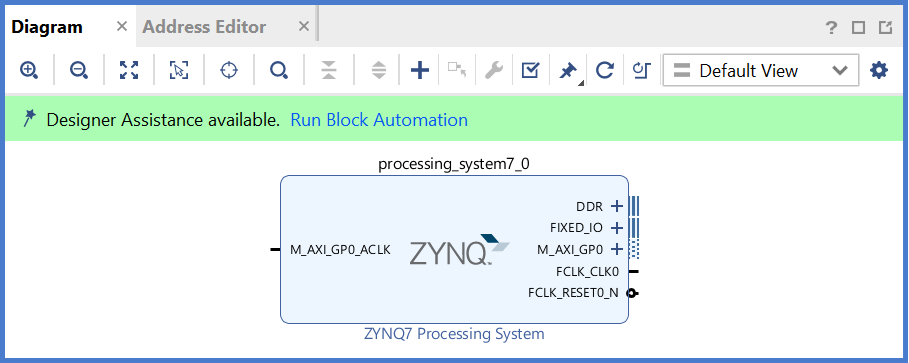
ZYNQ7 in block diagram
Configuring the Zynq-7000 Processing System with Presets in Vivado
In the Block Diagram window, notice the message stating that Designer assistance is available, as shown in the following figure.
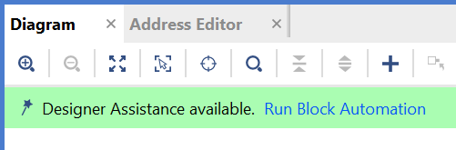
Click the Run Block Automation link. The Run Block Automation view opens.
Note that Cross Trigger In and Cross Trigger Out are disabled. For a detailed tutorial with information about cross trigger set-up, refer to the Vivado Design Suite Tutorial: Embedded Processor Hardware Design (UG940).
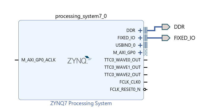
Click OK to accept the default processor system options and make default pin connections.
The automation result looks like this. It configures PS properties inside the block and connects fixed IO and DDR pins.
Validating the Design and Connecting Ports
Now, let’s validate the design.
Right-click in the white space of the Diagram window and select Validate Design. Alternatively, you can press the F6 key or the check button on the block diagram toolbar.
A critical message appears, indicating that the
M_AXI_GP0_ACLKmust be connected.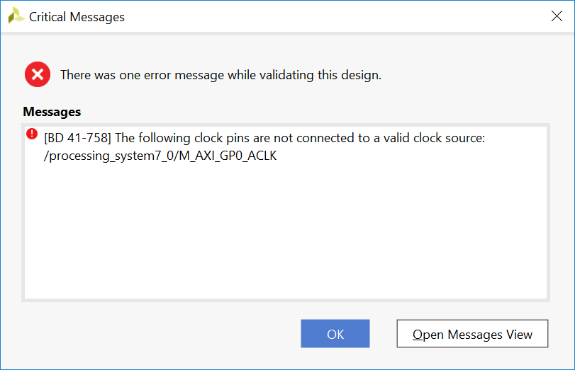
Click OK to close the message window.
Connect the
M_AXI_GP0_ACLKsignal to PS generated PL clock signal.The PS can generate four clock signals with
FCLK_CLK<number>. These are the clocks for the PL fabric. The clock frequency can be adjusted in PS block settings.In the Diagram window of the ZYNQ7 Processing System block, locate the M_AXI_GP0_ACLK port. Hover your mouse over the connector port until the pencil button appears.
Click the M_AXI_GP0_ACLK port and drag to the FCLK_CLK0 port to make a connection between the two ports.
Validate the design again to ensure there are no other errors.
Right-click in the white space of the Diagram window and select Validate Design.
A dialog box with the following message opens:
Validation successful. There are no errors or critical warnings in this design.
Click OK to close the message.
Creating an HDL Wrapper for the Block Diagram
Click the Sources window.
It should be in Hierarchy tab by default. If it’s not there, click the Hierarchy tab.
Expand Design Sources, right-click the block diagram file system(system.bd), and select Create HDL Wrapper.
The Create HDL Wrapper view opens. You will use this view to create an HDL wrapper file for the processor subsystem.
Tip
The HDL wrapper is a top-level entity required by the design tools.
Select Let Vivado manage wrapper and auto-update and click OK.
system_wrapper.vis generated. It is set to the top module of this design automatically.
Generating the Block Design
In Flow Navigator window, click Generate Block Design under IP Integrator.
Change the Synthesis Options to Global.
Note
If the synthesis option is Global, only wrapper files are generated during the block design generation phase, and the design will be synthesized as a whole at the synthesis stage. If the synthesis option is Out of context per IP or Out of context per Block design, the wrapper of the IP or block design will be generated and synthesized during block design generation, and the generated netlists will be combined together at the synthesis stage.
Click Generate.
This step builds all the required output products for the selected source. For example, constraints do not need to be manually created for the IP processor system. The Vivado tools automatically generate the XDC file for the processor subsystem when Generate Output Products is selected.
When the Generate Output Products process completes, click OK.
In the Sources window, click the IP Sources view. Here you can see the output products that you just generated, as shown in the following figure.
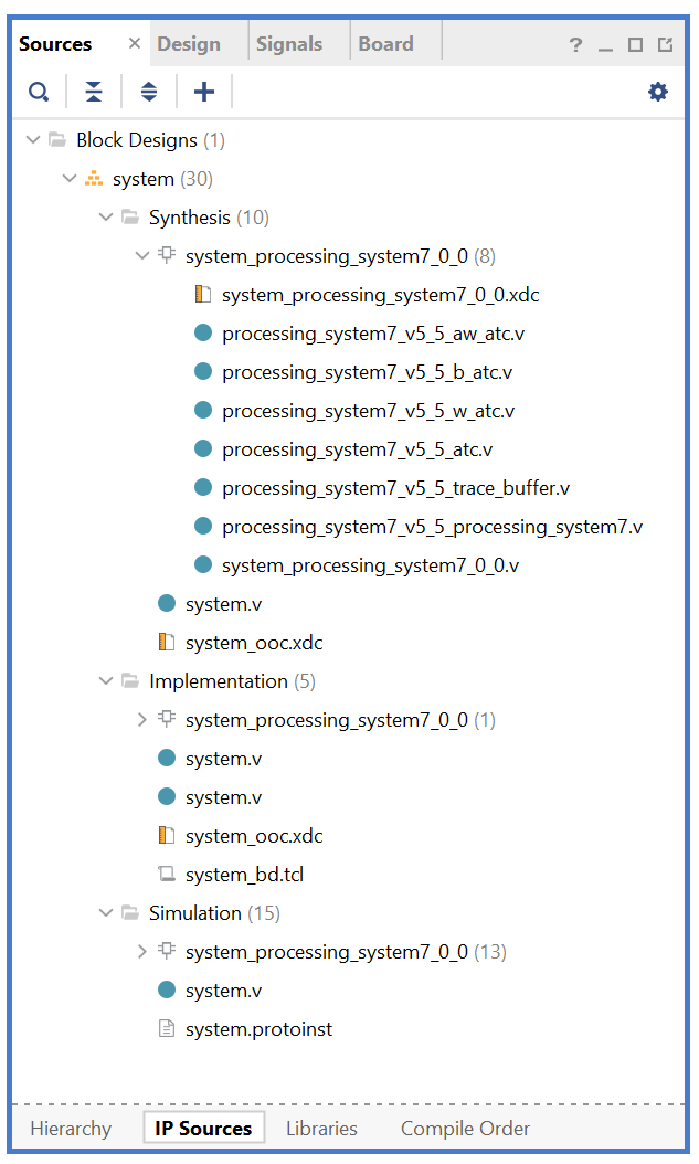
Generated IP Source Files
Exporting Hardware
Two types of hardware can be exported from Vivado: pre-synthesis and post-implementation. In the block design for this example, the hardware in the PL is the signal from FCLK_CLK0 to M_AXI_GP0_ACLK. It drives the clock of M_AXI_GP0. Because only pure PS functions will be tested in this example and PL resources will not be used, no loads are added to the M_AXI_GP0 AXI interface. You can skip the synthesis, implementation and bitstream generation phases to save time. We will export the pre-synthesis hardware in this case.
From the Vivado main menu, select File→ Export → Export Hardware. The Export Hardware Platform wizard opens.
Use the information in the following table to make selections in each of the wizard screens. Click Next wherever necessary.
Screen
System Property
Setting or Command to Use
Output Files
XSA file name Export to
Pre-synthesis. Leave as system_wrapper. Leave as C:/edt/edt_zc702.
Click Finish.
After a while, the Vivado Tcl Console reports the following message;
system_wrapper.xsais the exported hardware handoff file.write_hw_platform -fixed -force -file C:/edt/edt_zc702/system_wrapper.xsa INFO: [Vivado 12-4895] Creating Hardware Platform: C:/edt/edt_zc702/system_wrapper.xsa ... INFO: [Hsi 55-2053] elapsed time for repository (C:/Xilinx/Vivado/2021.2/data\embeddedsw) loading 1 seconds INFO: [Vivado 12-12467] The Hardware Platform can be used for Hardware INFO: [Vivado 12-4896] Successfully created Hardware Platform: C:/edt/edt_zc702/system_wrapper.xsa
What’s Next?
Now you can start developing the software for your project using the Vitis software platform. The next sections help you create a software application for your hardware platform.
Example 2: Creating and Running a “Hello World” Application
In this example, you will learn how to manage the board settings, make cable connections, connect to the board through your PC, and run a simple “Hello World” software application in JTAG mode using System Debugger in the Vitis IDE.
Input and Output Files
Input Files:
system_wrapper.xsaOutput Files:
hello_world.elf
Setting Up the Board
Connect the power cable to the board.
Connect the USB UART cable to J17.
Connect the USB JTAG cable:
Connect a micro USB cable between the host machine and the ZC702 target board U23. Be careful not to use J1 by mistake.
Make sure that the SW10 switch settings for JTAG selection are set to choose USB JTAG:
Bit-1 is 0
Bit-2 is 1
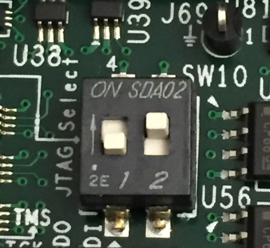
Note
0 = switch is open.
1 = switch is closed.
Setup JTAG boot mode using the switch indicated in the following figure.
Ensure that jumpers J27 and J28 are placed on the side farther from the SD card slot.
Change the SW16 switch setting as shown in the following figure.
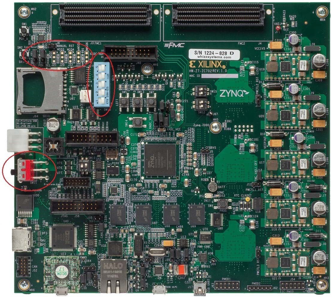
JTAG Boot Setup
Power on the ZC702 board.
Creating a Vitis Platform Project
Launch the Vitis IDE with any of the actions below:
From the Vivado IDE, select Tools -> Launch Vitis IDE.
On Windows, launch the Vitis IDE by using the desktop shortcut or Windows start menu → Xilinx Design Suite → Xilinx Vitis 2021.2.
On Linux, run
source <Vitis Installation Directory>/settings64.shto set up the environment and runvitis &.
Select the workspace location as C:/edt/edt_zc702_workspace or any given location path.
Vitis will create the workspace folder if it is not already created.
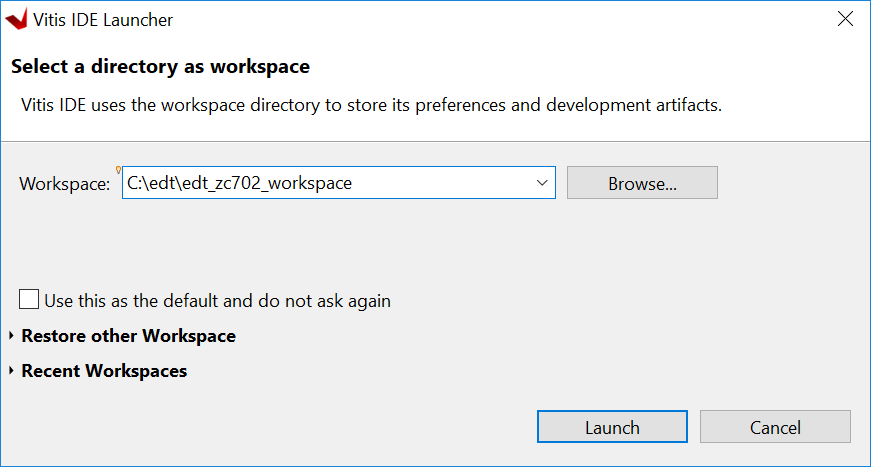
Vitis IDE Launcher
Click Launch. The Vitis IDE opens.
Review the Welcome page and close it.
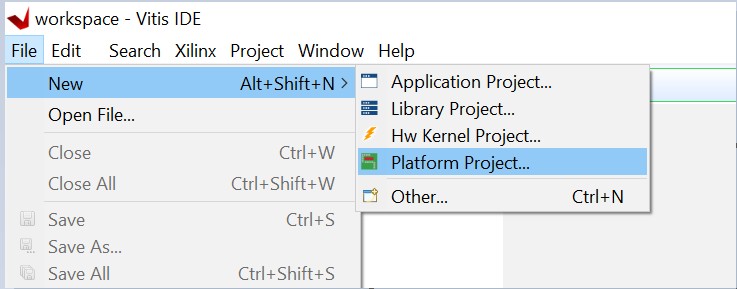
Click File → New → Platform Project to create a platform project from the XSA file generated by Vivado.
When the New Platform Project wizard opens, enter the platform project name as zc702_edt, as shown in following figure. Click Next.
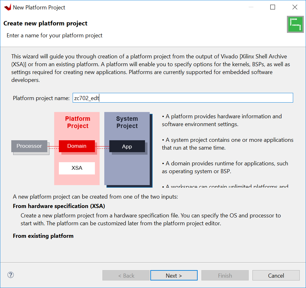
Platform Project Name
In the Platform page, you see the Create a new platform from hardware (XSA) tab by default. Under Hardware Specification, click browse to specify the XSA file
C:\edt\edt`\_zc702\system`\_wrapper.xsa\, and click OK.When the XSA file is selected, the Software Specification fields are updated so that the operating system is standalone and the processor is ps7_cortexa9_0.
Keep the Generate boot components option selected, as shown in the following figure.
Click Finish.
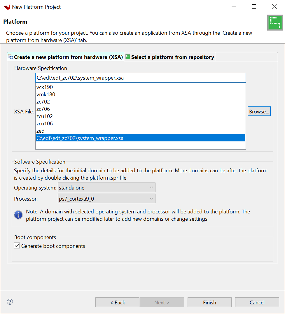
Select XSA
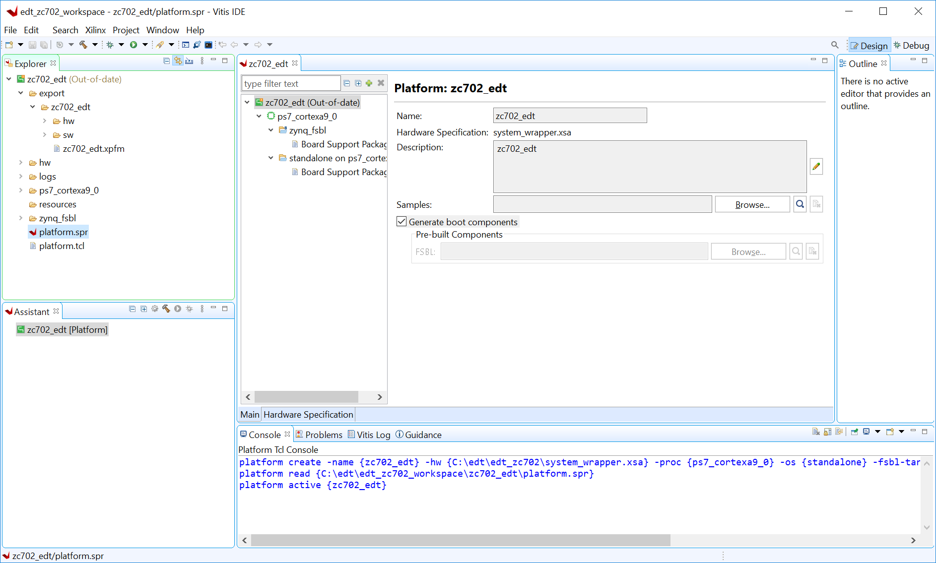
The platform project is created. In the Explorer view, double-click zc702_edt → platform.spr to view the platform view as shown in the following figure.
In the Explorer view, expand export → zc702_edt to find the exported Hardware Specification file,
system_wrapper.xsa(under thehwfolder), and the top-level platform XML file,zc702_edt.xpfm. Double-click on the XSA file to see the address map for the entire processing system, as shown in the following figure.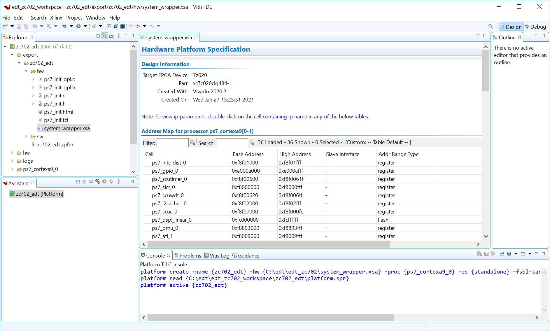
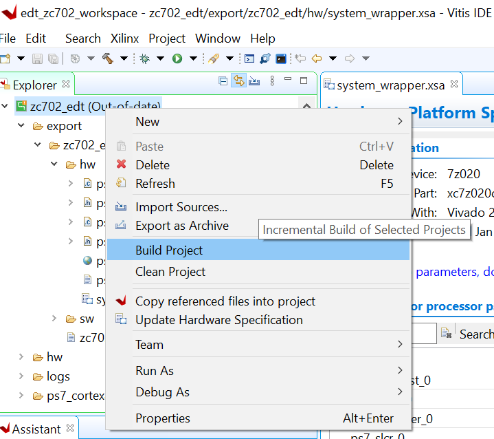
Build the platform project either by clicking the hammer button or by right-clicking on the platform project and selecting Build Project as shown in following figure.
Build Project
As the project builds, you can see the output in the Console window.
The build process takes some time because it is not only building the standalone BSP, but also boot components such as FSBL.
What Just Happened?
Using the Vitis IDE, you have created a platform project and exported the XSA file to the workspace in the C:\designs\workspace. The export operation generated a standalone domain with a ps7_cortexa9_0 processor and an FSBL application project. You have built a platform project, and the generated Xilinx platform definition file (zc702_edt.xpfm) can be used as a platform for the applications that you create in the Vitis IDE.
Creating the Hello World Application
Select File → New → Application Project.
The New Application Project wizard opens. Enable the option Skip welcome page next time and click Next.
Use the information in the following table to make your selections in the wizard screens.
Screen
System Properties
Setting or Command to Use
Platform
Select a platform from repository
Click zc702_edt [custom].
Application Project Details
Application project name
Enter hello_world.
System project name
Keep hello_world_system.
Target Processor
Keep ps7_cortexa9_0 selected.
Show all processors in hardware specification
Keep unchecked.
Domain
Select a domain
Keep standalone on ps7_cortex9_0 selected.
Templates
Available Templates
Hello World.
Click Finish. The Vitis software platform creates the hello_world application project and hello_world_system project in the Explorer view.
While entering the application project name, the Vitis IDE populates the system project name automatically with + “_system”. You are free to update the system project name if you wish.
By default, the New Application Wizard only shows the processors used by the domains in the platform. If you want to create a new platform during the application creation process, enable the Show all processors in hardware specification option.
Right-click the hello_world standalone application and select Build Project to generate the
hello_world.elfbinary file.
Running the Hello World Application on a ZC702 Board
Open a serial communication utility for the COM port assigned on your system.
The Vitis software platform provides a serial terminal utility will be used throughout the tutorial. You can also use your preferred serial terminal application.
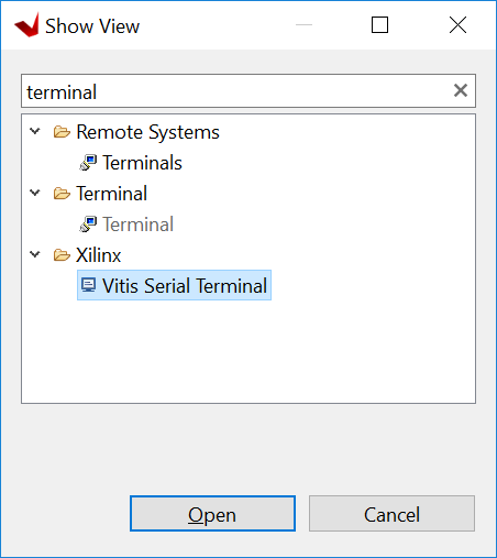
To open this utility, select Window → Show view.
In the Show View dialog box, type terminal in the search box.
Select Vitis Serial Terminal.
Click Open.
Open Vitis Serial Terminal
Click the Add button in the Vitis Serial Terminal to connect to a serial terminal.
Select the port from the dropdown menu.
Keep the Advanced Settings as-is.
Click OK
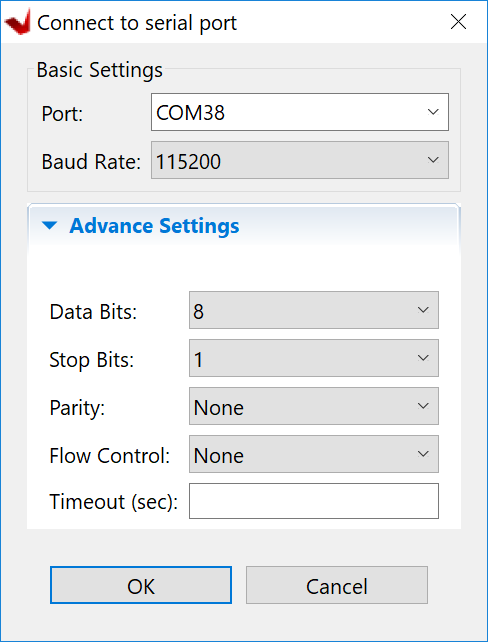
Connect UART
Right-click hello_world and select Run as → Run Configurations.
Right-click Single Application Debug and click New Configuration. The Vitis software platform creates the new run configuration, named Debugger_hello_world-Default.
The configurations associated with the application are pre-populated in the Main tab of the Run Configurations dialog box.
Click the Target Setup page and review the settings. The default choice is the Tcl script.
Click Run.
“Hello World” appears on the Vitis Serial Terminal, as shown in the following figure.
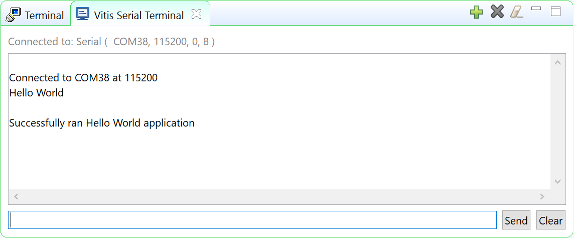
Terminal Print Result
Note
No bitstream download is required for the above software application to be executed on the Zynq SoC evaluation board. The Arm Cortex-A9 dual core is already present on the board. Basic initialization of this system to run a simple application is accomplished by the device initialization Tcl script.
What Just Happened?
The application software sent the “Hello World” string to the UART1 peripheral of the PS section.
From UART1, the “Hello World” string goes byte-by-byte to the serial terminal application running on the host machine, which displays it as a string.
Additional Information
Domain or Board Support Package
A domain or board support package (BSP) is a collection of software drivers and, optionally, the operating system on which to build your application. It is the support code for a given hardware platform or board that helps in basic initialization at power up and helps software applications to be run on top of it. You can create multiple applications to run on the domain. A domain is tied to a single processor in the platform.
Standalone OS
Standalone is a simple, low-level software layer. It provides access to basic processor features such as caches, interrupts, and exceptions, as well as the basic processor features of a hosted environment. These basic features include standard input/output, profiling, abort, and exit. It is a single-threaded semi-hosted environment.
The application you ran in this chapter was created on top of the standalone OS. The domain/BSP that your software application targets is selected during the New Platform Project creation process.
In the next chapter, you will learn how to debug software applications using the Vitis software platform.