AVED V80/V80P - Memory Resources
Overview
The AVED design contains discrete DDR, DDR DIMM, and HBM.
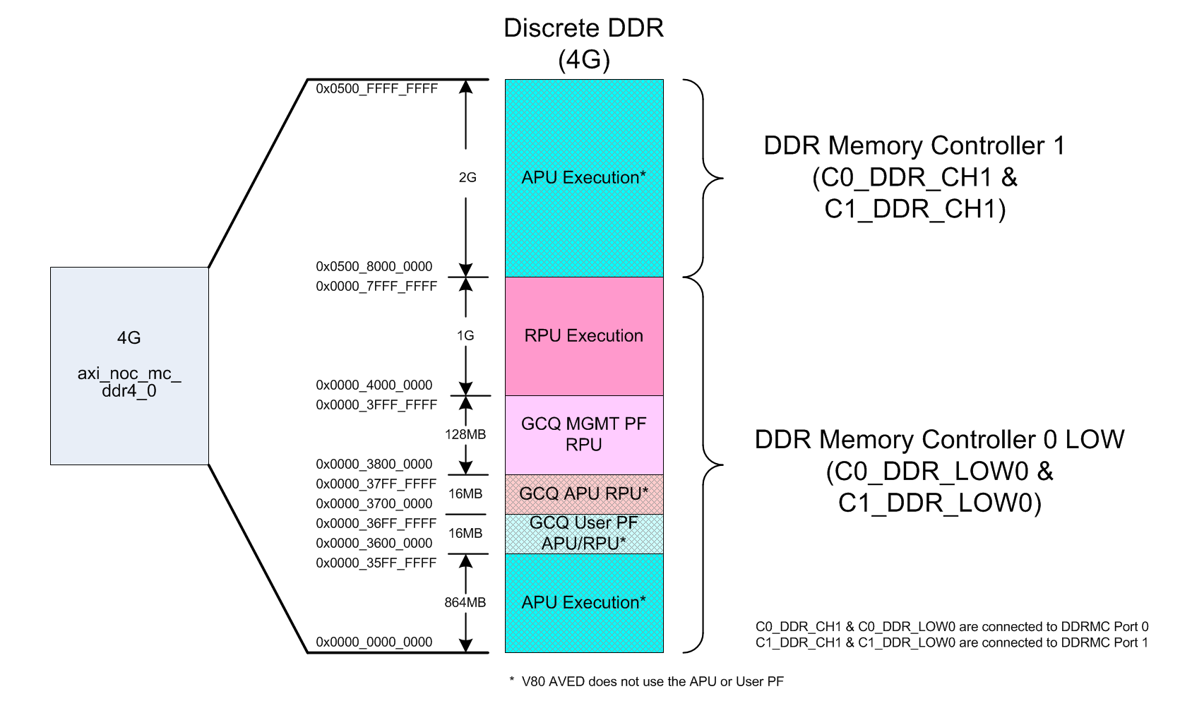
Discrete DDR
AVED contains 4GB of DDR that is used for APU and RPU execution, and inter-processor communication between the PMC, RPU, and APU via the general command queue (GCQ) IP. The DDR operates at 200MHz, and it is controlled by the AMD Versal™ integrated memory controller (DDRMC). This hardened MC contains four ports to optimize throughput to the DDR. The AVED design only uses MC Ports 0 and 1. The diagram below illustrates the organization of the DDR memory. AVED does not currently use a user PF or the APU, so those memory locations are not currently used (indicated by * in the below diagram with the cross-hatch background).
More information on the MC can be found here: https://docs.xilinx.com/r/en-US/pg313-network-on-chip/Integrated-Memory-Controller-DDRMC-Architecture.
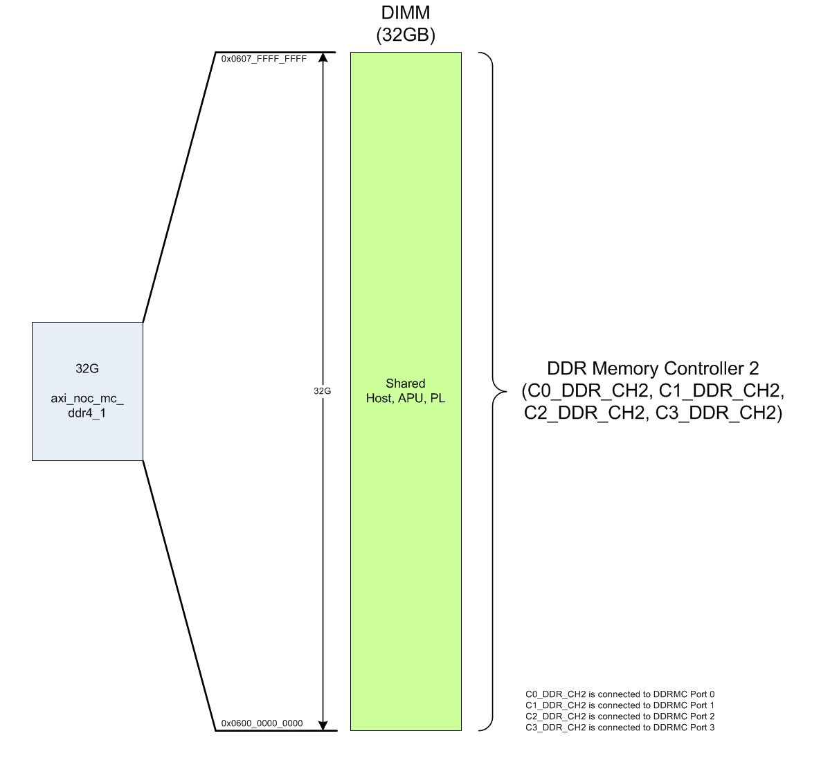
DDR DIMM (V80 only)
AVED V80 contains 32GB of DDR DIMM that is a shared memory resource for the host, APU, and programmable logic (PL). There is not any predefined organization or partitioning of this memory. Like the DDR, the DIMM operates at 200MHz and it is controlled by the Versal integrated memory controller (DDRMC). This hardened MC contains four ports to optimize throughput to the DDR. The AVED V80 design uses all four ports, but other connections to these ports are allowed. The diagram below illustrates the DIMM memory space. AVED V80 does not currently use the APU, but it is available for future growth. This DIMM is not available on the V80P card.
More information on the MC can be found at https://docs.xilinx.com/r/en-US/pg313-network-on-chip/Integrated-Memory-Controller-DDRMC-Architecture.
HBM
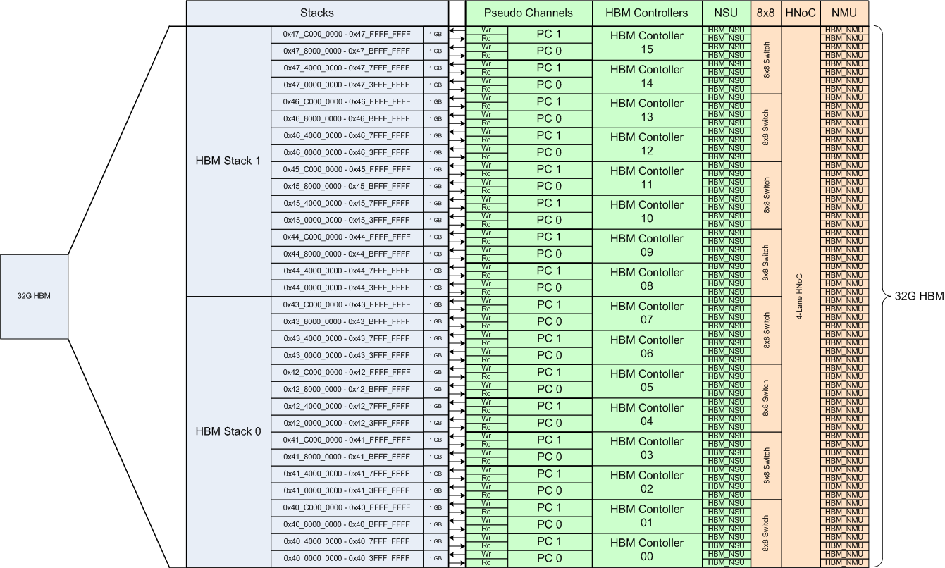
HBM memory is a high bandwidth, low power memory alternative to DDR. AVED contains 32GB of on-chip high-bandwidth memory (HBM). Like the DDR and DIMM, HBM operates at 200MHz. It is controlled by the Versal Integrated HBM controller. There is not any predefined organization or partitioning of this memory.
HBM is comprised of two 16GB stacks. Each stack has eight integrated AXI HBM Controllers. Each HBM controller contains two pseudo channels where each pseudo channel addresses a 1GB dedicated portion of the HBM. The HBM architecture also allows for global memory access to each master connected to the HBM; however accessing a non-direct portion of the memory will come at a performance cost.
More information on the HBM MC can be found at https://docs.xilinx.com/r/en-US/pg313-network-on-chip/Integrated-HBM-Controller.
Page Revision: v. 21