UL3524 Ultra Low Latency Trading |
PCIe DDR Reference Design: Simulation
Running the Simulation
To run a simulation of the design, follow the instructions detailed here.
DDR I2C Power Plane Enable
Simulation of enabling the DDR power plane via I2C is provided below. The waveform should run for approximately 1.5ms. At this time, a test complete message will appear in the log window.
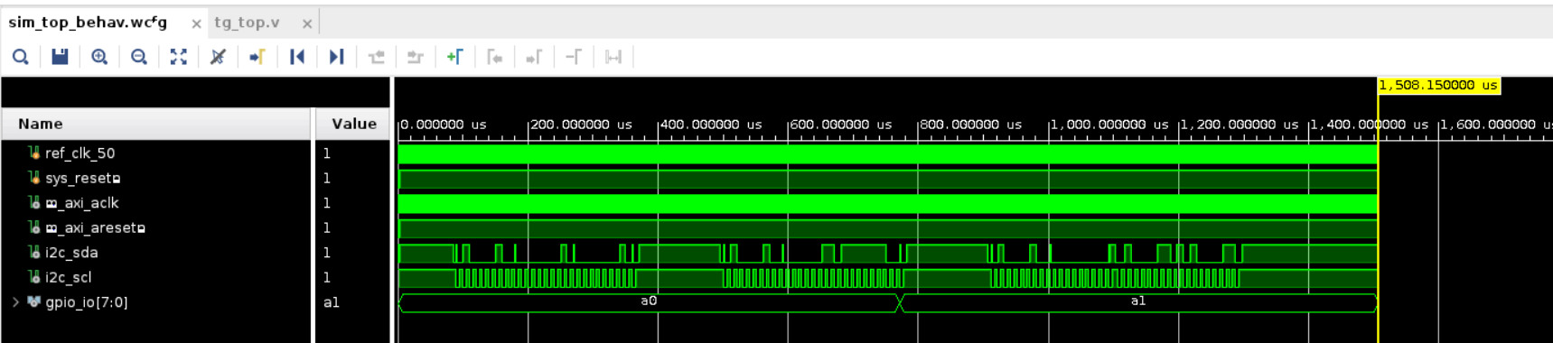
Figure: Waveform window consisting of the three I2C transfers.
Power Enable Transfer #1
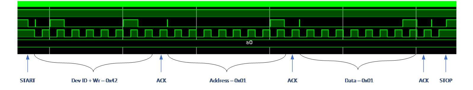
Figure: Set P0 output value to 1 (set bit 0 of register 0x1).
Power Enable Transfer #2
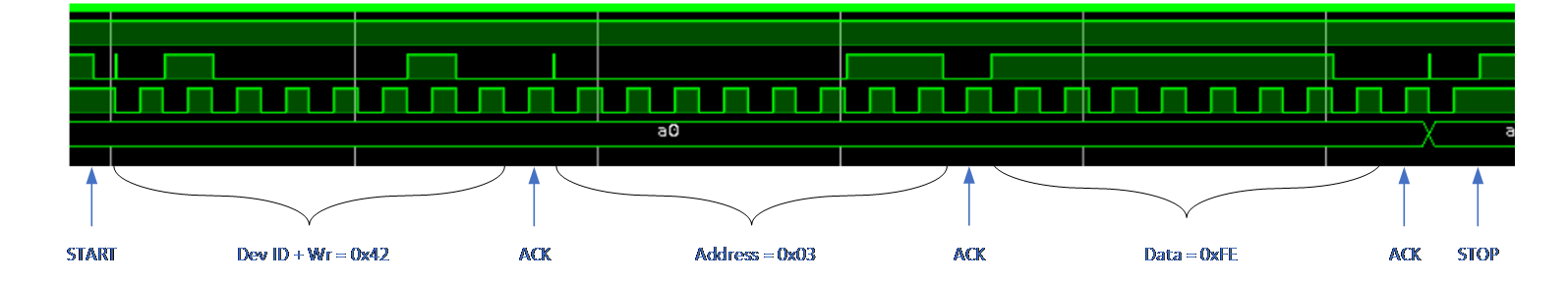
Figure: Set P0 to output mode (clear bit 0 of register 0x3).
Power Enable Transfer #3
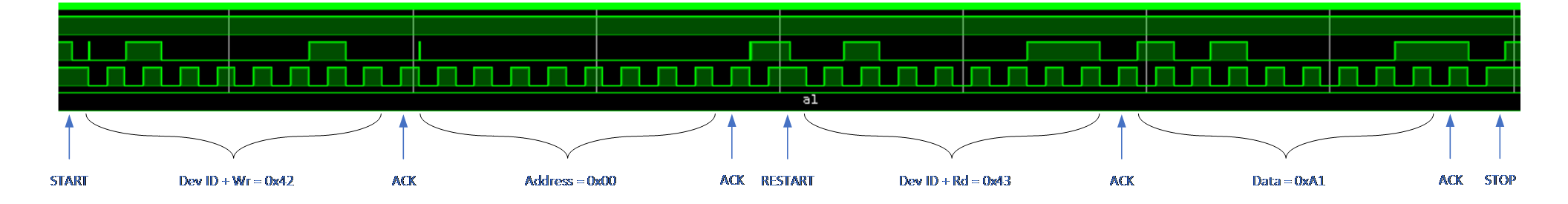
Figure: Read back register 0x0 which corresponds to value of P0 to P7. Bit 0 is set because of the previous transfers. Bits 7 and 5 are set because the simulation has these two pins connected to pull-ups.
Support
For additional documentation, please refer to the UL3524 product page and the UL3524 Lounge.
For support, contact your FAE or refer to support resources at: https://support.xilinx.com
Copyright © 2020–2023 Advanced Micro Devices, Inc