UL3524 Ultra Low Latency Trading |
QDRII+ MIG Reference Design: Simulation
Running the Simulation
To run a simulation of the design, follow the instructions detailed here.
Simulation Behavior
This section will outline the expected simulation behavior of the qdriip_ref_simple_tb. It will go through an example AXI write and read transaction and show the corresponding QDRII+ write and read operation.
Write
The following waveforms show an example of an AXI write to the memory address 0x0000_0008.
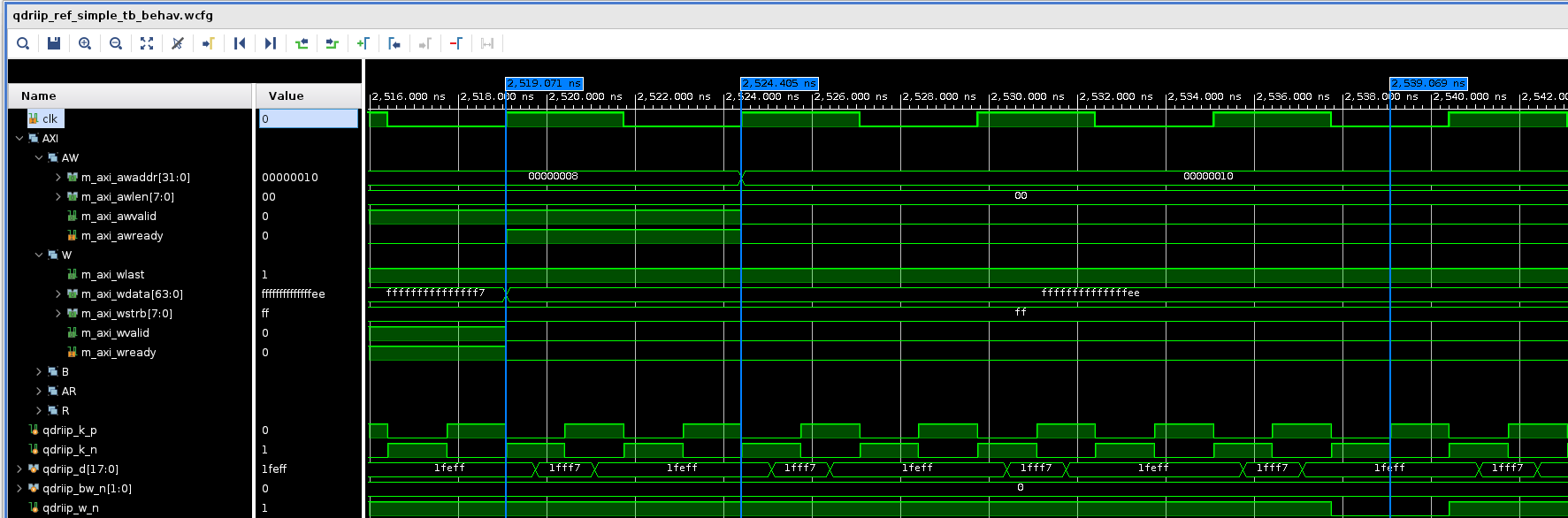
Figure: An example of AXI write address and data handshake and sampling of a QDRII+ write command. Starting from the leftmost marker:
Handshake of the write data m_axi_wdata[63:0] (0xffff_ffff_ffff_fff7)
Handshake of the write address m_axi_awaddr[31:0] (0x0000_0008)
Sampling of the corresponding QDRII+ write command qdriip_w_n on the posedge of qdriip_k_p
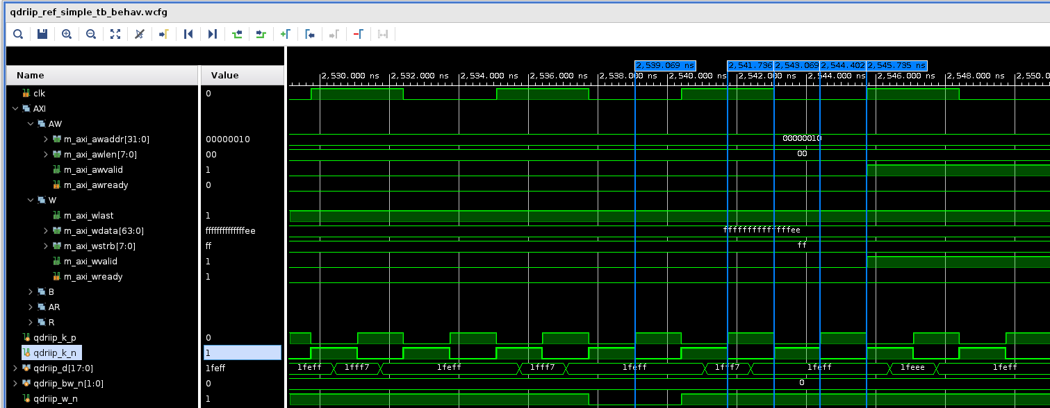
Figure: Waveform of the corresponding QDRII+ write operation (burst length: 4). Starting from the leftmost marker:
Sampling of the corresponding QDRII+ write command qdriip_w_n on the posedge of qdriip_k_p
Sampling of qdriip_d[17:0] (0x1_fff7) on the posedge of qdriip_k_p
Sampling of qdriip_d[17:0] (0x1_feff) on the posedge of qdriip_k_n
Sampling of qdriip_d[17:0] (0x1_feff) on the posedge of qdriip_k_p
Sampling of qdriip_d[17:0] (0x1_feff) on the posedge of qdriip_k_n
Note: Each byte of the AXI write data gets XOR’ed for an odd parity bit. E.g. 0xfff7 -> 0x1_fff7.
Read
The following waveforms show an example of an AXI read to the memory address 0x0000_0008.
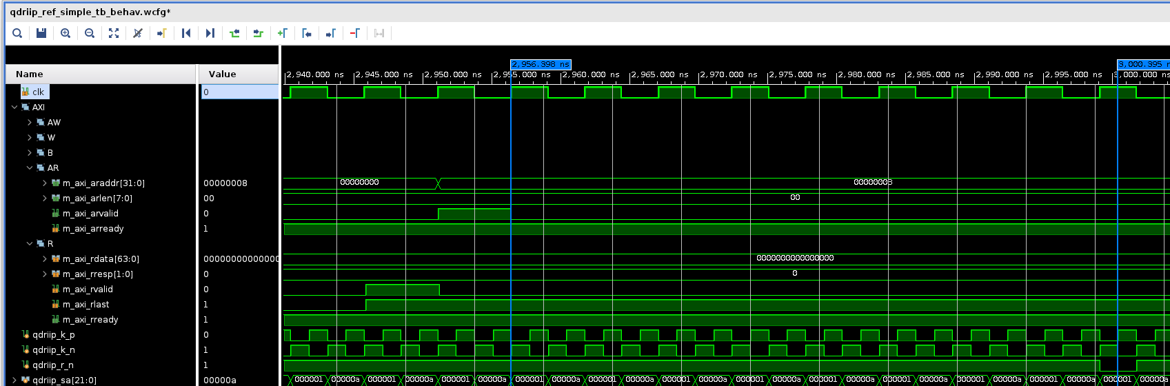
Figure: An example of AXI read address handshake and sampling of the corresponding QDRII+ read command. Starting from the leftmost marker:
Handshake of the read address m_axi_araddr (0x0000_0008).
Sampling of the corresponding QDRII+ read command qdriip_r_n with read address qdriip_sa[21:0] (0x00_0001) on the posedge of qdriip_k_p
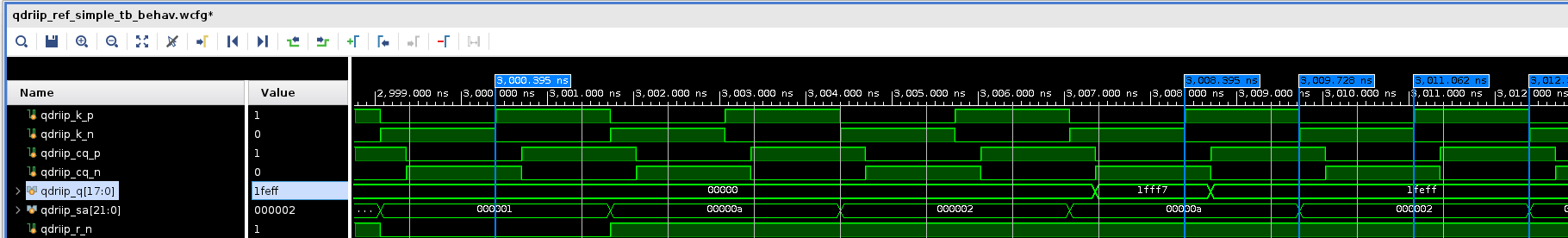
Figure: Waveform of the corresponding QDRII+ (burst length: 4) read operation. Starting from the leftmost marker:
Sampling of the corresponding QDRII+ read command qdriip_r_n with read address qdriip_sa[21:0] (0x00_0001) on the posedge of qdriip_k_p
Sampling of qdriip_q[17:0] (0x1_fff7) on the posedge of qdriip_k_p
Sampling of qdriip_q[17:0] (0x1_feff) on the posedge of qdriip_k_n
Sampling of qdriip_q[17:0] (0x1_feff) on the posedge of qdriip_k_p
Sampling of qdriip_q[17:0] (0x1_feff) on the posedge of qdriip_k_n
qdriip_cq_p/n are the echo clock returned from the memory derived from qdriip_k_p/n and are used as strobes.
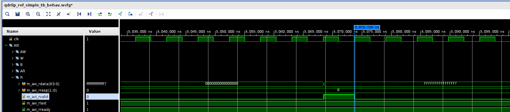
Figure: Waveform of the handshake of an AXI read data m_axi_rdata (0xffff_ffff_ffff_fff7).
Support
For additional documentation, please refer to the UL3524 product page and the UL3524 Lounge.
For support, contact your FAE or refer to support resources at: https://support.xilinx.com
Copyright © 2020–2023 Advanced Micro Devices, Inc